We have obtained experimental confirmation of the prediction that explosive crystallization of amorphous germanium proceeds via an intermediate melting step.
It is well known that the mechanical properties of thin films depend critically on film thickness However, the contributions from film thickness and grain size are difficult to separate, because they typically scale with each other. In one study by Venkatraman and Bravman, Al films, which were thinned using anodic oxidation to reduce film thickness without changing grain size, showed a clear increase in yield stress with decreasing film thickness. We have performed a similar study on both electroplated and sputtered Cu films by using chemical-mechanical polishing (CMP) to reduce the film thickness without changing the grain size. Stress-temperature curves were measured for both the electroplated and sputtered Cu films with thicknesses between 0.1 and 1.8 microns using a laser scanning wafer curvature technique. The yield stress at room temperature was found to increase with decreasing film thickness for both sets of samples. The sputtered films, however, showed higher yield stresses in comparison to the electroplated films. Most of these differences can be attributed to the different microstructures of the films, which were determined by focused ion beam (FIB) microscopy and x-ray diffraction.
Fine conducting features have been produced on Si and SiO2 substrates by irradiation of spin-on palladium acetate, [Pd(O2CCH3)2]3 films with a submicron focused ion beam. The exposures were made with a 20 keV Ga+, focused to a 0.2 micrometer spot. Electrical conductivity measurements were made on the resultant features as a function of ion dose for linewidths of one and ten micrometers. The sheet conductivity in the two cases was comparable and increased dramatically in the dose range between 2×10¹⁴ and 5×10¹⁴ ions/cm2. The conductivity of the exposed lines was further increased after heating in a hydrogen atmosphere. Measurements of carbon and oxygen content indicate that even at the highest ion doses a significant amount of organic material remains. Results are compared to those for 2 MeV He+ and Ne+ broad beam exposures. Potential applications are also discussed.
This paper reviews recent detailed investigations into the crystal growth kinetics and the microstructure of ion-beam-stimulated epitaxial crystallisation of silicon. Beam-induced crystallisation at temperatures between 200–400°C is found to be characterised by an activation energy of 0.24eV. Furthermore, in this temperature regime, crystal growth on (100) silicon is found to be free of extended defects except for a sharp hand of dislocation loops centred about the range of the ions employed to stimulate crystallisation. A higher temperature regime (>400°C) is observed in which the growth kinetics are less well defined but appear to be associated with an apparent activation energy of >0.5eV. In this regime, extended defects are observed to extend from the ion range to the surface. Results are presented which strongly suggest that nuclear energy deposition precisely at the amorphous-crystalline interface is responsible for crystallisation under ion irradiation. It is argued that the major fraction (2.4eV) of the thermal-only activation energy for epitaxial crystallisation of silicon is likely to be associated with the formation of nucleation sites for growth, a step which is achieved athermally under ion irradiation. In addition, the growth rate per unit ion fluence is found to be independent of substrate orientation at temperatures <450°C and independent of doping concentration for temperatures <400°C. These results are consistent with our proposed model for beam-induced crystallisation.
Electrically conducting palladium features have been produced by laser and ion beam irradiation of thin palladium acetate films. The photothermal reaction induced by scanned continuous wave Ar+ laser irradiation leads to metal lines that may exhibit periodic structure. This results from repeated propagation of “explosive” reaction fronts generated by coupling of the heat from the absorbed laser radiation with the heat of the decomposition reaction of the film. In contrast, 2 MeV He+ ion irradiation produces smooth metallic-looking features that contain up to 20% of the original carbon and 5% of the original oxygen content of the film. Films irradiated with 2 MeV Ne+ ions contain slightly lower amounts of carbon and oxygen residues, but fully exposed thick films (0.90 µm) appear black rather than metallic silver. In addition to having significantly higher purity, the laser-written features have lower resistivities than the ion beam-irradiated features. Infrared spectroscopy of the ion beam-irradiated films as a function of dose indicates a progressive loss in intensity of the characteristics acetate (COO−) vibrations. This occurs at doses lower than those associated with major C and O loss from the films. Partially ion-exposed films continue to decompose to metallic-looking material over a period of weeks after irradiation. Metallic palladium particles apparently catalyze this process.
The microstructure of materials (grain orientation, grain boundaries, grain size distribution, local strain/stress gradients, defects,...) is very important in defining the electromigration resistance of interconnect lines in modern integrated circuits. Recently, techniques have been developed for using submicrometer focused white and monochromatic x-ray beams at synchrotrons to obtain local orientation and strain information within individual grains of thin film materials. In this work, we use the x-ray microdiffraction beam line (7.3.3) at the Advanced Light Source to map the orientation and local stress variations in passivated Al(Cu) test structures (width: 0.7, 4.1 μm) as well as in Al(Cu) blanket films. The temperature effects on microstructure and stress were studied in those same structures by in-situ orientation and stress mapping during a temperature cycle between 25°C and 345°C. Results show large local variations in the different stress components which significantly depart from their average values obtained by more conventional techniques, yet the average stresses in both cases agree well. Possible reasons for these variations will be discussed.
The Panel was charged with assessing the present scientific understanding of the size-dependent physical and chemical properties of clusters, the methods of synthesis of macroscopic amounts of size-selected clusters with desired properties, and most importantly, the possibility of their controlled assembly into new materials with novel properties. The Panel was composed of both academic and industrial scientists from the physics, chemistry, and materials science communities, and met in January 1988.In materials (insulators, semiconductors, and metals) with strong chemical bonding, there is extensive spatial delocalization of valence electrons, and therefore the bulk physical properties which depend upon these electrons develop only gradually with cluster size. Recent research using supersonic-jet, gas-aggregation, colloidal, and chemical-synthetic methods indeed clearly establishes that intermediate size clusters have novel and hybrid properties, between the molecular and bulk solid-state limits. A scientific understanding of these transitions in properties has only been partially achieved, and the Panel believes that this interdisciplinary area of science is at the very heart of the basic nature of materials. In Sec. V (Future Challenges and Opportunities), a series of basic questions for future research are detailed. Each question has an obvious impact on our potential ability to create new materials.Present methods for the synthesis of useful amounts of size-selected clusters, with surface chemical properties purposefully controlled and/or modified, are almost nonexistent, and these fundamentally limit our ability to explore the assembly of clusters into potentially novel materials. While elegant spectroscopic and chemisorption studies of size-selected clusters have been carried out using molecular-beam technologies, there are no demonstrated methods for recovery and accumulation of such samples. Within the past year, the first reports of the chemical synthesis of clusters with surfaces chemically modified have been reported for limited classes of materials. Apparatus for the accumulation and consolidation of nanophase materials have been developed, and the first promising studies of their physical properties are appearing. In both the chemical and nanophase synthesis areas, clusters with a distribution of sizes and shapes are being studied. Progress on macroscopic synthetic methods for size-selected clusters of controlled surface properties is the most important immediate goal recognized by the Panel. Simultaneous improvement in physical characterization will be necessary to guide synthesis research.Assuming such progress will occur, the Panel suggests that self-assembly of clusters into new elemental polymorphs and new types of nanoscale heterogeneous materials offers an area of intriguing technological promise. The electrical and optical properties of such heterogeneous materials could be tailored in very specific ways. Such ideas are quite speculative at this time; their implementation critically depends upon controlled modification of cluster surfaces, and upon development of characterization and theoretical tools to guide experiments.The Panel concluded that a number of genuinely novel ideas had been enunciated, and that in its opinion some would surely lead to exciting new science and important new materials.
In this study we present investigation on the anelastic behavior of sputtered 1 [.proportional]m thin Cu films. Most of the literature that reports on the mechanical properties of thin metallic films is based on substrate curvature measurements. We have developed a new version of a bulge tester that combines the capacitive measurement of the bulge deflection of a membrane with a resonance frequency measurement of the residual stress in the membrane. A Cu membrane is plastically deformed to a pre-determined strain by controlled gas-pressure bulging of the membrane. After the bulging stress is removed, the residual tensile stress, which has been decreased by the plastic deformation, is then determined by measuring the resonant frequency as a function of time. Immediately after plastic straining, the residual (tensile) stress of membranes was observed to increase. At room temperature a maximum stress was typically reached in the order of an hour. At still longer times the stress decreased again as a result of creep. The transient increase in stress following plastic straining grew larger as the amount of plastic strain produced by bulging was increased. With higher temperatures the transient became both faster and larger. A model is presented that based on the mechanism of thermally activated glide separates the microstructure in a class of “soft” and “hard” grains solving the issue of an “apparent” increase in strain energy as a function of time after deformation.
The international reactor innovative and secure (IRIS) is a modular pressurized water reactor with an integral configuration (all primary system components - reactor core, internals, pumps, steam generators, pressurizer, and control rod drive mechanisms - are inside the reactor vessel). The IRIS plant conceptual design was completed in 2001 and the preliminary design is currently underway. The pre-application licensing process with the United States Nuclear Regulatory Commission (USNRC) started in October 2002.The first line of defense in IRIS is to eliminate event initiators that could potentially lead to core damage. If it is not possible to eliminate certain accidents altogether, then the design inherently reduces their consequences and/or decreases their probability of occurring. One of the most obvious advantages of the IRIS Safety-by-Design (TM) approach is the elimination of large break loss-of-coolant accidents (LBLOCAs), since no large primary penetrations of the reactor vessel or large loop piping exist.While the IRIS Safety-by-Design (TM) approach is a logical step in the effort to produce advanced reactors, the desired advances in safety must still be demonstrated in the licensing arena. With the elimination of LBLOCA, an important next consideration is to show the IRIS design fulfills the promise of increased safety also for small break LOCAs (SBLOCAs). Accordingly, the SBLOCA phenomena identification and ranking table (PIRT) project was established. The primary objective of the IRIS SBLOCA PIRT project was to identify the relative importance of phenomena in the IRIS response to SBLOCAs. This relative importance, coupled with the current relative state of knowledge for the phenomena, provides a framework for the planning of the continued experimental and analytical efforts.To satisfy the SBLOCA PIRT project objectives, Westinghouse organized an expert panel whose members were carefully selected to insure that the PIRT results reflect internationally recognized experience in reactor safety analysis, and were not biased by program preconceptions internal to the IRIS program.The SBLOCA PIRT Panel concluded that continued experimental data and analytical tool development in the following areas, in decreasing level of significance, are perceived as important with respect to satisfying the safety analysis and licensing objectives of the IRIS program: (1) steam generator; (2) pressure suppression system, containment dry well and their interactions; (3) emergency heat removal system; (4) core, long-term gravity makeup system, automatic depressurization system, and pressurizer; (5) direct vessel injection system and reactor vessel cavity. (c) 2006 Elsevier B.V. All rights reserved.
Scanning X-ray microdiffraction (microSXRD) combines the use of high-brilliance synchrotron sources with the latest achromatic X-ray focusing optics and fast large-area two-dimensional-detector technology. Using white beams or a combination of white and monochromatic beams, this technique allows for the orientation and strain/stress mapping of polycrystalline thin films with submicrometer spatial resolution. The technique is described in detail as applied to the study of thin aluminium and copper blanket films and lines following electromigration testing and/or thermal cycling experiments. It is shown that there are significant orientation and strain/stress variations between grains and inside individual grains. A polycrystalline film when investigated at the granular (micrometer) level shows a highly mechanically inhomogeneous medium that allows insight into its mesoscopic properties. If the microSXRD data are averaged over a macroscopic range, results show good agreement with direct macroscopic texture and stress measurements.
Grain-to-grain interactions dominate the plasticity of Al thin films and establish effective length scales smaller than the grain size. We have measured large strain distributions and their changes under plastic strain in 1.5-microm-thick Al 0.5% Cu films using a 0.8-microm-diameter white x-ray probe at the Advanced Light Source. Strain distributions arise not only from the distribution of grain sizes and orientation, but also from the differences in grain shape and from stress environment. Multiple active glide plane domains have been found within single grains. Large grains behave like multiple smaller grains even before a dislocation substructure can evolve.
The partitioning of potentially-toxic metals into coexisting minerals, the difficulty of identifying the mineral species to which these elements are bound, and the multiplicity of sorption mechanisms are key problems in understanding how metals interact at the molecular level with environmental nanoparticles.These long-standing impediments are now yielding to investigations by X-ray techniques developed at 3rd generation synchrotron facilities.We shall show that these problems can be overcome without disrupting the heterogeneous matrix by combining scanning X-ray fluorescence (SRXF) and diffraction (SXRD), and extended X-ray absorption fine structure (EXAFS) spectroscopy at micrometer-scale of resolution.First, micro-SXRF and micro-SXRD are used to identify the host solid phase by mapping the distributions of elements and solid species, respectively.Micro-EXAFS spectroscopy is then used to determine the mechanism of trace element binding by the host phase at the molecular scale.To illustrate the complementary application of these three techniques, we studied how nickel is sequestered in soil ferromanganese nodules, a hellishly complex natural matrix consisting of submicrometer to nanometer-sized particles with varying structure and chemical composition.We showed that nickel substitutes for Mn (III) in the manganese layer of the MnO 2-Al(OH)3 mixed-layer oxide lithiophorite.The affinity of Ni for lithiophorite was characteristic of micronodules sampled from soils across the USA and Europe.Since many natural and synthetic materials are heterogeneous at nanometer to micrometer scales, the synergistic use of micro-SXRF, micro-SXRD, and micro-EXAFS is expected to have broad applications to earth and materials science.
The advent of third generation synchrotron light sources in combination with x-ray focusing devices such as Kirkpatrick-Baez mirrors make Lane diffraction on a submicron length scale possible. Analysis of Laue images enables us to determine the deviatoric part of the 3D strain tensor to an accuracy of 2x10(-4) in strain with a spatial resolution comparable to the grain size in our thin films. In this paper the application of x-ray microdiffraction to the temperature dependence of the mechanical behavior of a sputtered blanket Cu film and of electroplated damascene Cu lines will be presented. Microdiffiraction reveals very large variations in the strain of a film or line from grain to grain. When the strain is averaged over a macroscopic region the results are in good agreement with direct macroscopic stress measurements. However, the strain variations are so large that in some cases in which the average stress is tensile there are some grains actually under compression. The full implications of these observations are still being considered, but it is clear that the mechanical properties of thin film materials are now accessible with new visibility.
We have used scanning white beam x-ray microdiffraction to study microstructural evolution during an in situ electromigration experiment on a passivated Al(Cu) test line. The data show plastic deformation and grain rotations occurring under the influence of electromigration, seen as broadening, movement, and splitting of reflections diffracted from individual metal grains. We believe this deformation is due to localized shear stresses that arise due to the inhomogeneous transfer of metal along the line. Deviatoric stress measurements show changes in the components of stress within the line, including relaxation of stress when current is removed.
The availability of high brilliance synchrotron sources, coupled with recent progress in achromatic focusing optics and large area two-dimensional detector technology, has allowed us to develop an x-ray synchrotron technique that is capable of mapping orientation and strain/stress in polycrystalline thin films with submicron spatial resolution. To demonstrate the capabilities of this instrument, we have employed it to study the microstructure of aluminum thin film structures at the granular and subgranular levels. Due to the relatively low absorption of x-rays in materials, this technique can be used to study passivated samples, an important advantage over most electron probes given the very different mechanical behavior of buried and unpassivated materials.
At the Advanced Light Source in Berkeley we have instrumented a beam line that is devoted exclusively to X-ray micro-diffraction problems. By micro-diffraction we mean those classes of problems in Physics and Materials Science that require X-ray beam sizes in the sub-micron range. The instrument is for instance, capable of probing a sub-micron size volume inside micron-sized aluminum metal grains buried under a silicon dioxide insulating layer. The resulting Laue pattern is collected on a large area CCD detector and automatically indexed to yield the grain orientation and deviatoric (distortional) strain tensor of this sub-micron volume. A four-crystal monochromator is then inserted into the beam, which allows monochromatic light to illuminate the same part of the sample. Measurement of the diffracted photon energy allows for the determination of d spacings. The combination of white and monochromatic beam measurements allow for the determination of the total strain/stress tensor (6 components) inside each sub-micron-sized illuminated volume of the sample.
The transition from sputtered Al to electroplated Cu interconnects for future microelectronic devices has led to an interest in understanding the relationships between the microstructure and texture of Cu that might impact electrical performance, similar to what has been done for Al. Electroplated Cu undergoes a recrystallization at room temperature that is related to the presence of organic and inorganic additives in the plating bath. As plated, the Cu grains are small (approx. 0.1 μm) and equiaxed, but over a period of hours to days, recrystallization results in grains several microns in size. We observe a significant weakening of the strong as-plated (111) texture by x-ray diffraction pole figure measurements and an increase in the level of randomness. We propose that multiple twinning is the leading mechanism for this phenomenon.
We report a comparison of the room temperature recrystallization of electroplated (EP) copper in blanket films as a function of thickness measured by focused ion beam (FIB) microscope images and sheet resistance measurements. Both sets of data show an increase in rate with film thickness from 0.75νm up to 5νm, while little recrystallization is observed in films thinner than 0.75νm. Interestingly, the recrystallization rates from FIB analysis are consistently faster than those from the sheet resistance measurements. These data suggest that the recrystallization is initiated close to the top surface of the EP Cu film, but that in thinner films a high surface-to-volume ratio allows surface inhibition or pinning to retard the transformation. A Johnson-Mehl-AvramiKolmogorov (JMAK) analysis of the two data sets yields unusually high values for the Avrami exponent μ of up to 7 for the FIB data, while lower values of around 4 are obtained for the sheet resistance data. X-ray diffraction pole figures of the films have also been collected and correlations between the crystallographic texture, film thickness and recrystallization are discussed.
An X-ray microdiffraction dedicated beamline, combining white and monochromatic beam capabilities, has been built at the Advanced Light Source. The purpose of this beamline is to address the myriad problems in Materials Science and Physics that require submicron x-ray beams for structural characterization. Many such problems are found in the general area of thin films and nano-materials. For instance, the ability to characterize the orientation and strain state in individual grains of thin films allows us to measure structural changes at a very local level. These microstructural changes are influenced heavily by such parameters as deposition conditions and subsequent treatment. The accurate measurement of strain gradients at the micron and sub-micron level finds many applications ranging from the strain state under nano-indenters to gradients at crack tips. Undoubtedly many other applications will unfold in the future as we gain experience with the capabilities and limitations of this instrument. We have applied this technique to measure grain orientation and residual stress in single grains of pure Al interconnect lines and preliminary results on post-electromigration test experiments are presented. It is shown that measurements with this instrument can be used to resolve the complete stress tensor (6 components) in a submicron volume inside a single grain of Al under a passivation layer with an overall precision of about 20 MPa. The microstructure of passivated lines appears to be complex, with grains divided into identifiable subgrains and noticeable local variations of both tensile/compressive and shear stresses within single grains.
The microstructure of narrow metal conductors in the electrical interconnections on IC chips has often been identified as of major importance in the reliability of these devices. The stresses and stress gradients that develop in the conductors as a result of thermal expansion differences in the materials and of electromigration at high current densities are believed to be strongly dependent on the details of the grain structure. The present work discusses new techniques based on microbeam x-ray diffraction (MBXRD) that have enabled measurement not only of the microstructure of totally encapsulated conductors but also of the local stresses in them on a micron and submicron scale. White x-rays from the Advanced Light Source were focused to a micron spot size by Kirkpatrick-Baez mirrors. The sample was stepped under the micro-beam and Laue images obtained at each sample location using a CCD area detector. Microstructure and local strain were deduced from these images. Cu lines with widths ranging from 0.8 μm to 5 μm and thickness of 1 μm were investigated. Comparisons are made between the capabilities of MBXRD and the well established techniques of broad beam XRD, electron back scatter diffraction (EBSD) and focused ion beam imagining (FIB).
 Louis Lanzerotti合作论文数Center for Solar-Terrestrial Research, New Jersey Institute of Technology40
 Robert E. Johnson合作论文数School of Engineering and Applied Science, University of Virginia38
 W.M. Augustyniak合作论文数18Jw Boring合作论文数17C.T. Reimann合作论文数16Jm Poate合作论文数14
 Ralph Spolenak合作论文数Laboratory for Nanometallurgy, Eidgenossische Technische Hochschule Zurich;Department of Materials, Eidgenossische Technische Hochschule Zurich12David L Barr合作论文数12K.J. Marcantonio合作论文数11BC Valek合作论文数10
 Howard Padmore合作论文数Lawrence Berkeley National Laboratory10
 Nobumichi Tamura合作论文数Advanced Light Source, Lawrence Berkeley National Laboratory10
 Robert Elliman合作论文数Physics Education Centre, Research School of Physics, Australian National University;Department of Electronic Materials Engineering, Research School of Physics, Australian National University;Department of Nuclear Physics & Accelerator Applications, Research School of Physics, Australian National University9
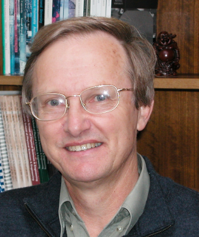 Jim Williams合作论文数College of Science, Australian National University;Acton Semiconductors (Aust) Pty Ltd;Research School of Physical Sciences and Engineering, Australian National University9
 Jan Linnros合作论文数KTH Royal Institute of Technology9Richard Celestre合作论文数Advanced Light Source;Lawrence Berkeley National Laboratory;Lawrence Berkeley National Laboratory9
 John Bravman合作论文数Materials Science & Engineering Department, Stanford University9Me Gross合作论文数8
 Martin F. Jarrold合作论文数Department of Chemistry, The College of Arts + Sciences, Indiana University Bloomington8
 Alastair MacDowell合作论文数Lawrence Berkeley National Laboratory8B. W. Batterman合作论文数7Jr Patel合作论文数7
 George K. Celler合作论文数University of Wisconsin-Madison7d e grosjean合作论文数7
 Thirumalai Venky Venkatesan合作论文数Center for Quantum Research and Technology, Dodge Family College of Arts and Sciences, University of Oklahoma;Neocera and Neocera Magma6dale conrad jacobson合作论文数5Ee Chaban合作论文数5Tt Sheng合作论文数5Dm Maher合作论文数5
 Yves Chabal合作论文数Erik Jonsson School of Engineering and Computer Science, University of Texas Dallas5
 Douglas B. Chrisey合作论文数School of Science & Engineering, Tulane University;Department of Physics and Engineering Physics, Tulane University;Department of Biomedical Engineering, Tulane University5
 Raul a Baragiola合作论文数Laboratory for Atomic and Surface Physics, University of Virginia5
 And Valerio Pirronello合作论文数Dipartimento di Metodologie;Fisiche e Chimiche per l'Ingegneria;Universita ' di Catania;Dipartimento di Metodologie|Fisiche e Chimiche per l'Ingegneria, Universita ' di Catania5HJ LEAMY合作论文数5J. W. Garrett合作论文数5Thomas N. Marieb合作论文数5c lingk合作论文数4Wo Sprenger合作论文数4M. E. Gross合作论文数4ME Geusic合作论文数4Cherry a Murray合作论文数4
 Atsushi Ogura (小椋厚志)合作论文数School of Science and Technology, Undergraduate School, Meiji University4G. Foti合作论文数4R.V. Knoell合作论文数4
 Marek Sosnowski合作论文数4
 Krishnan Raghavachari合作论文数Department of Chemistry, The College of Arts and Sciences, Indiana University4
 Louis E. Brus (路易斯·布鲁斯)合作论文数Department of Chemistry, Columbia University4C. G. Maclennan合作论文数4
 Lloyd R. Harriott合作论文数4




