The paper describes the essential requirements of the Electrostatic Discharge (ESD) EDA verification flow to be aligned within the IC design community. The proposed flow offers a systematic approach to check ESD robustness across all IC blocks during the product definition, chip architecture, main module and full IC design phases, and during the final IC verification. This flow is substantiated by case studies of key ESD checks at different IC design stages, demonstrating the necessity of replacing manual checks with EDA tool enabled verification.
This work investigates the robustness of a stacked or cascoded driver under electrostatic discharge (ESD) events. Using output driver circuits in an actual I/O system with predrivers and rail-based power clamps, the impacts of all possible predriver connections and stacked-driver sizing are examined with the very fast transmission line pulse. It is verified that, when the input of the predriver connected to the top MOSFET is grounded, the failure current (IT2) is improved by ~ 110%, compared to the worst case where both predriver inputs are tied to VDD. Also, a simple trigger circuit which guarantees the electrical connection for better ESD immunity is proposed.
Silicon-controlled rectifier (SCR) devices are used as local clamping ESD devices. However, conventional designs suffer from slow turn-on, which causes problems in sub 10 ns charged-device model (CDM) protection, especially in deeply scaled technologies. In this paper, a double-well field-effect diode (DWFED) and an improved field-effect diode (FED) are designed to address this challenge. They are fabricated and characterized in 45 nm silicon-on-insulator (SOI) technology and experimentally demonstrated to be suitable for pad-based local clamping under a normal supply voltage (Vdd) range (at or below 1 V) in high-speed applications. ESD protection capabilities are investigated using very fast transmission line pulse (VF-TLP) tests to predict the device performance in CDM events. FED’s advantages in improving transient turn-on behavior and reducing DC leakage current are analyzed and compared with the regular SCR and the DWFED. Technology CAD (TCAD) simulations are used to interpret turn-on behavior and guide design. The improved devices may be implemented in a local clamping scheme that expands the ESD design window for advanced technology nodes.
This paper focuses on the characterization, modeling, and design of electrostatic discharge (ESD) protection devices such as the gated diode, the bulk substrate diode, and the double-well field-effect diode (DWFED) in 45 nm silicon-on-insulator technology. ESD protection capabilities are investigated using very fast transmission line pulsing tests to predict a device's performance in charged device model (CDM) ESD events. Device capacitance, which is critical for high-speed input/output performance, is evaluated, and biasing schemes and processing techniques are proposed to reduce the parasitic capacitance during normal operating conditions. Technology computer-aided design simulations are used to interpret the physical effects. The implementation of devices for meeting CDM protection requirements is discussed. Evaluation results identify DWFED as a promising candidate for the pad-based local-clamping scheme.
This work investigates the ESD robustness of stacked drivers in bulk and SOI technologies. The impact of stacked driver sizing and pre-driver connection is examined in detail using VF-TLP and TLP measurement. It is shown that proper pre-driver configuration can double V-t2, thereby improving I/O's I-t2.
In this paper, the FER is shown to be a possible candidate for ESD protection in deeply scaled SOI technology. It2 of above 50 mA/μm and capacitance below 0.6 fF/μm are achieved. Despite the FER's higher resistivity than SOI diode, its major advantage is the dual-directional current shunting capability, such that ESD protection between I/O pads and power buses can be achieved with a single-device solution at the pad instead of several devices. Therefore, this device expands the conventional ESD design space for trading off parameters such as resistivity, Ileak and capacitance. Results from measurements and TCAD simulations further instantiate the advantages of the FERs in current and future SOI technologies. For future technologies such as ultra-thin-film SOI and FinFET, better gate controllability can be achieved to sustain the inversion regions. Thus, the well doping can be increased to lower the resistivity, making the FER more suitable for I/O protection.
In this paper, the improved field-effect diode (FED) has been characterized and modeled in 45 nm silicon-on-insulator (SOI) technology. It has been experimentally shown to be suitable for pad-based local clamping under normal supply voltage (V dd ) range (below 1 V) in high-speed integrated circuits. ESD protection capabilities are investigated using very fast transmission line pulse (VF-TLP) tests to predict the device's performance in charged device model (CDM) ESD events. The FED's advantages in improving transient turn-on behavior and reducing DC leakage current have been analyzed and compared with other silicon-controlled-rectifier (SCR)-based SOI device variations. Technology CAD (TCAD) simulations are used to interpret the turn-on behavior and the physical effects. Process tradeoffs have been evaluated. The work prepares the device for being directly applied to high-speed input/output (I/O) circuit and it addresses the severe challenge in CDM ESD protection. The improved device enables the adoption of local clamping scheme that expands the ESD design window.
Challenges of design window shrinkage in deeply scaled silicon technologies are addressed by improving design, characterization, and modeling of I/O and ESD devices, and by developing ESD robustness and circuit performance co-design methodologies. Advanced ESD metrology methods are reviewed and their applications in providing key information for reliability modeling are investigated. Package and wafer level CDM correlation issues are examined.
In this paper, we present a comparison of the turn-on voltage between SOI-SCR, and the novel DWFED structure. We show that DWFED can achieve faster turn-on, protecting the low voltage devices more effectively. Using the pulse waveforms, we justify the use of a gate trigger circuit for the DWFED to reduce the transient spikes under faster CDM pulses.
This work focuses on characterization, modeling, and design of three different ESD protection devices for high-speed I/O applications in 45 nm silicon on insulator (SOI) technology. In this paper, the gated diode, the bulk substrate diode, and a double-well field-effect diode are evaluated using very fast transmission line pulse (VF-TLP) test method.
A simple indoor recirculating system for production of juvenile sea cucumber (Apostichopus japonicus) was operated on a commercial scale for 90 days during winter. The system consists of three 70m3 sea cucumber rearing tanks and one biofilter tank where macroalgae (Ulva pertusa) was used as a biofilter in order to reduce water requirements. Effluent from the sea cucumber tanks drained into the macroalgae biofilter tank and were then returned to the sea cucumber tanks by a discontinuous-flow recirculation system. Survival and growth rates in the sea cucumber culture tanks were similar to those in the control tank (with one water exchange per day). The survival rate averaged about 87%. The average body weight increased from 3.5±0.3g to 8.1±0.8g and total sea cucumber biomass production over the experimental period was 745gm−2 after initial stocking densities of 375gm−2. The growth rate of U. pertusa was 3.3%day−1. U. pertusa was efficient in removing toxic ammonia and in maintaining the water quality within acceptable levels for sea cucumber culture; there were only small daily variations of temperature, pH and DO. The U. pertusa tank removed 68% of the TAN (total ammonia-nitrogen) and 26% of the orthophosphate from the sea cucumber culture effluent; the macroalgae biofilter removed ammonia at an average rate of 0.459gNm−2day−1. It would be efficient to use the U. pertusa biofilter in a recirculating system for production of A. japonicus juveniles in winter.
Two numerical models based on the impedance field method have been implemented to investigate the flicker noise in MOSFETs with high-kappa gate stacks. The equivalent model uses approximate channel current noise source, while the physical model is based on the Langevin approach and accounts for the non-local carrier tunneling. The scaling impact on the flicker noise is investigated with the developed models. The validity of the models in the sub-threshold regime is examined. Comparison with experimental data indicates the importance of modeling the nonuniform trap energy distribution. The degradation of the flicker noise performance due to halo doping is also studied
This paper uses advanced TCAD tools to investigate the scaling effects on noise and linearity performance of analog RF MOS devices, as well as the implications on modeling those effects at the compact level. Impedance field method and hydrodynamic transport model are used to study the thermal noise behavior in aggressively scaled MOS devices. A flicker noise model is implemented; low frequency noise performance of devices based on alternative high-k gate dielectrics is also evaluated. The large signal distortion analysis is conducted based on the harmonic balance technique. The effects of doping profiles and their changes with technology scaling on the distortion performance are examined.
A developmentally retarded mutant (drm1) was identified from ethyl methanesulfonate (EMS)-mutagenized M2 seeds in Columbia (Col-0) genetic background. The drm1 flowers 109 d after sowing, with a whole life cycle of about 160 d. It also shows a pleiotropic phenotype, e.g., slow germination and lower germination rate, lower growth rate, curling leaves and abnormal floral organs. The drm1 mutation was a single recessive nuclear mutation, which was mapped to the bottom of chromosome 5 and located within a region of 20-30 kb around MXK3.1. There have been no mutants with similar phenotypes reported in the literature, suggesting that DRM1 is a novel flowering promoting locus. The findings that the drm1 flowered lately under all photoperiod conditions and its late flowering phenotype was significantly restored by vernalization treatment suggest that the drm1 is a typical late flowering mutant and most likely associated with the autonomous flowering pathway. The conclusion was further confirmed by the revelation that the transcript level of FLC was constantly upregulated in the drm1 at all the developmental phases examined, except for a very early stage. Moreover, the transcript levels of two other important repressors, EMF and TFL1, were also upregulated in the drm1, implying that the two repressors, along with FLC, seems to act in parallel pathways in the drm1 to regulate flowering as well as other aspects of floral development in a negatively additive way. This helps to explain why the drm1 exhibits a much more severe late-flowering phenotype than most late-flowering mutants reported. It also implies that the DRM1 might act upstream of these repressors.
In an attempt to screen stay-green mutants in Arabidopsis in the absence of light, a mutant displaying the characteristics of brassinosteroids mutants was isolated. This mutant, dst6, carries a single recessive mutation. Using molecular genetic markers, the mutation was mapped to the bottom of chromosome II , which is around the region of DET2 ,one of the genes known to cause brassinosteroids mutation. The analysis of cDNA and genomic sequence of DET2 in dst6 revealed a frame-shifting insertion. These results suggest that dst6 is a putative new allele of det2.
 Robert Dutton合作论文数Electrical Engineering Department, Stanford University9
 Jung-Hoon Chun合作论文数7
 Akram A. Salman合作论文数Advanced Micro Devices, One AMD Place7
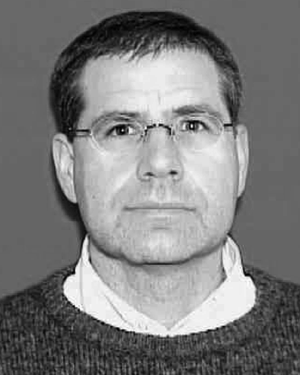 Mario M. Pelella合作论文数advanced micro devices5
 Yang Liu (刘旸)合作论文数College of Information Science & Electronic Engineering, Zhejiang University4
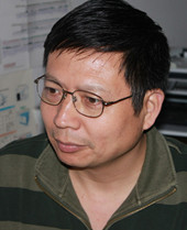 Benke Kuai (蒯本科)合作论文数School of Life Sciences, Fudan University3Yong Zhu (朱勇)合作论文数2Hongjun Zhou (周红军)合作论文数2Qiaoting Xu合作论文数2Kee-Won Kwon合作论文数1warren r anderson合作论文数1Kun Qian合作论文数1Fang Yu (俞芳)合作论文数1
 Chuanxin Qin (秦传新)合作论文数South China Sea Fisheries Research Institute, Chinese Academy of Fishery Sciences1Eunji Choi合作论文数1
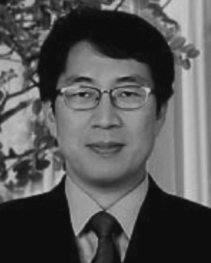 Gi-Doo Lee合作论文数1
 Harald Gossner合作论文数Intel Deutschland1
 Xiaofei Yu (于肖飞)合作论文数School of Life Sciences, Fudan University1
 Yingliang Liu (刘应亮)合作论文数College of Materials and Energy, South China Agricultural University1
 Jun Ding (丁君)合作论文数College of Fisheries and Life Science, Dalian Ocean University;National Demonstration Center for Experimental Aquaculture Education, Dalian Ocean University1Hua Wang (王华)合作论文数1
 Guodong Ren (任国栋)合作论文数School of Life Sciences, Fudan University1M. Etherton合作论文数1Yajun Cao合作论文数1
 Tze Wee Chen合作论文数1Michael G. Khazhinsky合作论文数Motorola, Inc.1
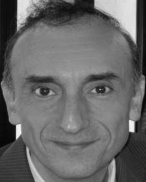 Gianluca Boselli合作论文数1Peter Griffin合作论文数1Tianlei Liu合作论文数1O. Tornblad合作论文数1




