Glial immunity plays a pivotal role in the maintenance of nervous system homeostasis and in responses to stress conditions, including neural injuries. The transcription factor Stat92E is activated independently of the canonical JAK/STAT pathway in Drosophila glial cells after brain injury to shape glial reactivity toward degenerating axons. However, the upstream regulatory mechanisms governing Stat92E activation remain elusive. Here, we reveal that selective autophagy gates nuclear translocation of Stat92E after injury and directs the degradation of the PIAS SUMO ligase family member Stat92E repressor, Su(var)2-10, in glia. Autophagic elimination of Su(var)2-10 mediated by its colocalization and interaction with the core autophagy factor Atg8a is required for efficient Stat92E-dependent transcription after injury. In line with this, we demonstrate that autophagy is essential for the up-regulation of an innate immune pathway in glial cells after axon injury, characterized by the induction of virus-induced RNA 1 (vir-1). We propose that autophagic Su(var)2-10 breakdown controls Stat92E activation to allow glial reactivity. These findings identify a critical role of autophagy in glial immunity as part of nervous system injury responses.
Glial immunity plays a pivotal role in the maintenance of nervous system homeostasis and responses to stress conditions, including neural injuries. In Drosophila melanogaster, the transcription factor Stat92E is activated in glial cells following central nervous system injury, independently of the canonical JAK/STAT pathway, to shape glial reactivity towards degenerated axons. However, the upstream regulatory mechanisms governing Stat92E activation remain elusive. Here, we reveal a selective autophagy-mediated regulation of Stat92E in glia by the degradation of the Stat92E repressor Su(var)2-10, a member of the PIAS SUMO ligase family. Atg8a, a core autophagy factor co-localizes and interacts with Su(var)2-10. Su(var)2-10 elimination is required for efficient Stat92E-dependent transcription after injury. Furthermore, we demonstrate that autophagy is essential for the upregulation of immune pathways, exemplified by virus-induced RNA 1 (vir-1), in glial cells following axon injury. We propose that Stat92E function is gated both by activating phosphorylation and autophagic Su(var)2-10 breakdown to licence glial reactivity. These findings underscore the critical role of autophagy in glial immunity and its potential impact on neural injury responses. ### Competing Interest Statement The authors have declared no competing interest.
Abstract Background The long-term safety and efficacy of repeated applications of subliminal transscleral cyclophotocoagulation (SL-TSCPC) with a focus on cumulative energy was evaluated in glaucoma patients. Methods In this retrospective, multicentric study the data of a total of 82 eyes with various causes of glaucoma that were treated with a single or multiple applications of SL-TSCPC were collected. Treatments were performed under general or local anesthesia with an 810 nm diode laser. Power was 2000 mW; duty cycle, 31.3%; total treatment duration, 80–320 s; equaling a total energy of 50–200 J per treatment session. Fifty-five eyes (55 patients) presented for all follow-ups, and these eyes were selected for further statistical analysis. The mean age was 60.0 ± 17.1 years, and 22 (40%) of the patients were female. Intraocular pressure (IOP) and dependence on further glaucoma medication were evaluated at 12 months following the initial treatment. Results Eyes underwent 1 or 2 consecutive SL-TSCPC treatments. Median (min–max) baseline IOP of 34 (13–69) decreased to 21.5 (7–61), 22 (8–68), 20 (9–68), and 19.5 (3–60) mmHg at the 1, 3, 6, and 12-month postoperative timepoints respectively. The mean (± SD) IOP decrease at 12 months was 26 ± 27%, 39 ± 32%, and 49 ± 33% in the low (below 120 J, n = 18), medium (120–200 J, n = 24), and high (above 200 J, n = 13) cumulative energy groups respectively. At the 12-month timepoint, oral carbonic anhydrase use was discontinued in ¾ of the cases. Conclusions It was found that the repeated application of SL-TSCPC safely and efficiently decreases IOP in a Caucasian population with heterogenous causes of glaucoma, eyes with silicone oil responded to a greater extent. Inclusion of cumulative energy scales may contribute to better addressing repeated procedures in a standardized fashion.
Le potentiel des matériaux 2D pour des applications dans les transistors à effet de champ présenté sur la base de simulations de transport quantique d’électrons basés sur la théorie de la fonctionnelle de la densité, les fonctions localisées de Wannier et la fonction de Green hors équilibre. Il en résulte un aperçu détaillé et des perspectives claires.
Glial engulfment of neuron-derived debris after trauma, during development, and in neurodegenerative diseases supports nervous system functions. However, mechanisms governing the efficiency of debris degradation in glia have remained largely unexplored. Here we show that LC3-associated phagocytosis (LAP), an engulfment pathway assisted by certain autophagy factors, promotes glial phagosome maturation in the Drosophila wing nerve. A LAP-specific subset of autophagy-related genes is required in glia for axon debris clearance, encoding members of the Atg8a (LC3) conjugation system and the Vps34 lipid kinase complex including UVRAG and Rubicon. Phagosomal Rubicon and Atg16 WD40 domain-dependent conjugation of Atg8a mediate proper breakdown of internalized axon fragments, and Rubicon overexpression in glia accelerates debris elimination. Finally, LAP promotes survival following traumatic brain injury. Our results reveal a role of glial LAP in the clearance of neuronal debris in vivo, with potential implications for the recovery of the injured nervous system.
In the nervous system, dead cell-derived material arising from injuries and neurodegeneration is normally removed by the phagocytic activity of macrophages or glia. Failure in this process can lead to excessive inflammation and secondary neurodegeneration. During phagocytosis, engulfed material is captured into phagosomes. Maturation and subsequent fusion of these vesicles with lysosomes may utilize components of the macroautophagy pathway that has been referred to as LC3-associated phagocytosis or LAP for short.
Two-dimensional (2D) materials are particularly attractive to build the channel of next-generation field-effect transistors (FETs) with gate lengths below 10-15 nm. Because the 2D technology has not yet reached the same level of maturity as its Silicon counterpart, device simulation can be of great help to predict the ultimate performance of 2D FETs and provide experimentalists with reliable design guidelines. In this paper, an ab initio modelling approach dedicated to well-known and exotic 2D materials is presented and applied to the simulation of various components, from thermionic to tunnelling transistors based on mono- and multi-layer channels. Moreover, the physics of metal - 2D semiconductor contacts is revealed and the importance of different scattering sources on the mobility of selected 2D materials is discussed. It is expected that modeling frameworks similar to the one described here will not only accompany future developments of 2D devices, but will also enable them.
This chapter discusses the potential of 2D materials as field-effect transistors from a modeling perspective, starting from the key features of monolayers. It introduces the importance of being able to simulate their electrical characteristics. The first 2D material under the ab initio microscope is MoS 2 ; the transition metal dichalcogenides (TMD) whose monolayer form was initially shown to provide excellent transistor characteristics is described in Radisavljevic et al. Besides TMDs, other 2D materials suitable for logic applications have emerged over the years, starting with black phosphorus: a monolayer of phosphorus atoms with a buckled honeycomb lattice. One of the key challenges 2D materials are facing is their contact with metallic electrodes. 2D materials do not only face challenges, they also offer opportunities in advanced logic applications. Their excellent electrostatic control properties are particularly appealing for the realization of band-to-band tunneling field-effect transistors.
Histone variants are different from their canonical counterparts in structure and are encoded by solitary genes with unique regulation to fulfill tissue or differentiation specific functions. A single H4 variant gene (His4r or H4r) that is located outside of the histone cluster and gives rise to a polyA tailed messenger RNA via replication-independent expression is preserved in Drosophila strains despite that its protein product is identical with canonical H4. In order to reveal information on the possible role of this alternative H4 we epitope tagged endogenous H4r and studied its spatial and temporal expression, and revealed its genome-wide localization to chromatin at the nucleosomal level. RNA and immunohistochemistry analysis of H4r expressed under its cognate regulation indicate expression of the gene throughout zygotic and larval development and presence of the protein product is evident already in the pronuclei of fertilized eggs. In the developing nervous system a slight disequibrium in H4r distribution is observable, cholinergic neurons are the most abundant among H4r-expressing cells. ChIP-seq experiments revealed H4r association with regulatory regions of genes involved in cellular stress response. The data presented here indicate that H4r has a variant histone function.
SQSTM1/p62-type selective macroautophagy/autophagy receptors cross-link poly-ubiquitinated cargo and autophagosomal LC3/Atg8 proteins to deliver them for lysosomal degradation. Consequently, loss of autophagy leads to accumulation of polyubiquitinated protein aggregates that are also frequently seen in various human diseases, but their physiological relevance is incompletely understood. Here, using a genetically non-redundant Drosophila model, we show that specific disruption of ubiquitinated protein autophagy and concomitant formation of polyubiquitinated aggregates has hardly any effect on bulk autophagy, proteasome activity and fly healthspan. We find that accumulation of ref(2)P/SQSTM1 due to a mutation that disrupts its binding to Atg8a results in the co-sequestering of Keap1 and thus activates the cnc/NFE2L2/Nrf2 antioxidant pathway. These mutant flies have increased tolerance to oxidative stress and reduced levels of aging-associated mitochondrial superoxide. Interestingly, ubiquitin overexpression in ref(2)P point mutants prevents the formation of large aggregates and restores the cargo recognition ability of ref(2)P, although it does not prevent the activation of antioxidant responses. Taken together, potential detrimental effects of impaired ubiquitinated protein autophagy are compensated by the aggregation-induced antioxidant response.
Since the first exfoliation of graphene and other transition metal dichalcogenides (TMDs), two-dimensional (2D) monolayers have seen an increasing number of applications. After investigating individual compounds, researchers have started to stack them as Lego bricks and create so-called van der Waals materials (vdWMs), which can be homo-or heterojunctions of 2D monolayers. The combination of an n-type and p-type 2-D material allows for example to realize atomically thin p-n diodes that can emit light [1] . By adding gate contacts to such vdWMs, the tunneling window between both monolayers can be modulated, giving rise to band-to-band tunneling field-effect transistors, a class of logic switches with potentially ultra-low power consumption [2] .
We experimentally demonstrate phase-sensitive fibre optic parametric amplification with gain >10dB and optical noise figure below 3dB for 11 channels spaced of 100 GHz. We employ all-fibre dispersion management to achieve a wideband phase-matching between signals and their copies.
2D transition metal dichalcogenide based van der Waals materials are promising candidates to realize tunnel field effect transistors (TFETs) with a steep subthreshold swing (SS) for low-power applications. Their atomically flat, self-passivated layers offer potentially defect free interlayer tunneling. There are still several issues that need to be addressed to experimentally achieve a steep SS, e.g., the Schottky contacts, impact of thick layers, and device architecture with respect to gate configuration. This paper resolves these challenges by experimentally demonstrating MoS2/MoTe2 TFETs and their electrical characteristics, in conjunction with ab initio simulations and surface Kelvin probe microscopy. The Schottky barrier's effect at the contact regions are isolated by fabricating individual buried gates below the contacts. Devices with different top and bottom gate configurations are produced to understand the impact of gate placement on the heterostructure characteristics. Quantum transport simulations are performed on MoS2/MoTe2 multilayer stack to evaluate the impact of multiple layers on TFET performance, effect of gate placement, and the mechanism behind indirect tunneling over the heterojunction region. This work highlights the influence of the Schottky contacts, multiple layers and the role of different gate configurations on the band-to-band tunneling phenomenon in 2D heterojunction TFETs.
Plantations of non-native trees for commercial use are common practice in Europe.They are known to have severe ecological impacts on arthropod fauna by altering microclimatic conditions and reducing microhabitat diversity. However, the effect of plantation tree species on winter-active fauna is relatively unknown. Spiders are a diverse predatory arthropod taxon with strong effect on their prey populations. The composition of spider communities sensitively indicates changes in habitat structure. We established 40 sampling sites in five non-native pine and five native poplar plantations and collected spiders with pitfall traps for two winters in the Southern part of Hungary. We assessed the average height of vegetation and percentage cover of leaf litter, mosses, herbaceous vegetation, and shrubs to characterize habitat structure. We found species richness and activity density of spiders in the non-native compared to the native plantations, presumably due to the more temperate microclimate in pine than in poplar plantations. However, there was no significant effect of habitat structure and its interaction with forest type on species richness and activity density of spiders. Species composition of non-native and native plantation forests differed significantly. Furthermore, we identified six characteristic spider species of non-native plantations with preference for relatively moist habitat conditions.The single characteristic species, (Agroeca cuprea Menge, 1873) for the native plantations preferred dry and partly shaded habitats. We conclude that the effect of microclimatic differences and prey availability presumably overrides the effect of habitat structure on winter- active spiders.
Due to their remarkable properties, single-layer 2-D materials appear as excellent candidates to extend Moore's scaling law beyond the currently manufactured silicon FinFETs. However, the known 2-D semiconducting components, essentially transition metal dichalcogenides, are still far from delivering the expected performance. Based on a recent theoretical study that predicts the existence of more than 1800 exfoliable 2-D materials, we investigate here the 100 most promising contenders for logic applications. Their current versus voltage characteristics are simulated from first-principles, combining density functional theory and advanced quantum transport calculations. Both n- and p-type configurations are considered, with gate lengths ranging from 15 down to 5 nm. From this large collection of electronic materials, we identify 13 compounds with electron and hole currents potentially much higher than those in future Si FinFETs. The resulting database widely expands the design space of 2-D transistors and provides original guidelines to the materials and device engineering community.
In the search for post Si CMOS transistors, different device geometries (FinFETs-on-oxide, nanowires, nanosheets), materials (III-V, Ge, carbon nanotubes), and combination of them have been receiving a lot of attention from the semiconductor industry and from academia. Recently, very promising experimental results have put 2-D single-layer crystals under the spotlight, starting from graphene in 2005 and followed by transition metal dichalcogenides (TMDs), e.g. MoS2 in 2011. Their excellent electrostatic properties, absence of surface dangling bonds, tuneable effective masses and band gaps, and possibility to be stacked on top of each other to form van der Waals heterostructures make 2-D materials particularly appealing for future logic applications, especially at gate lengths below 20 nm. A recent theoretical study based on density functional theory (DFT) [1] predicted that more than 1,800 2-D monolayer compounds might exist, with about 1,000 of them that could be relatively easily exfoliated from their 3-D parents. Among them, some exhibit semiconducting, other metallic or insulating behaviours. Still, it can be expected that hundreds could be suitable as channel material of future ultra-scaled transistors. Exploring the "current vs. voltage" characteristics of all of them to identify the ones that might eventually challenge the current Si FinFET technology is currently not possible at the experimental level: this would require the fabrication of very high number of samples that it would be difficult to compare to each other. Furthermore, the results might strongly depend on the crystal quality, processing techniques, measurement setups, or experimental conditions. All these effects do not allow to properly and unambiguously determine the intrinsic potential of each considered 2-D material. As an alternative, device simulation could be used to support the on-going experimental activity and guide it towards the best material-structure configurations. For that purpose, an accurate, physics-based modelling approach is necessary that does not take fitting parameters as inputs. Ab initio quantum transport solvers lend themselves perfectly to this type of exploratory studies. Such an advanced computer aided design (CAD) tool has been developed to evaluate the figures of merits (ON-current, injection velocity, inversion charge, sub-threshold slope, scalability, energy-delay product...) of future transistors relying on 2-D channel materials [2]. It combines plane-wave DFT calculations, transformations into maximally localised Wannier functions, constructions of device Hamiltonian matrices, and quantum transport simulations. By doing so, a full-band treatment of any single- or multi-layer 2-D compound is possible, without the need for a model parameterisation, as encountered in (semi-)empirical methods such as tight-binding or pseudo-potentials. Here, the properties of conventional TMDs and black phosphorus will be first simulated at the ab initio level and compared to those of strained-Si and III-V FinFETs. Since all theses device configurations will be investigated with the same tool (self-consistent Schrödinger and Poisson solver) and set of approximations, the results do not depend on the simulator features, but only on the intrinsic characteristics of each structure. As next step, the study will be extended by adding the data obtained for 100 other 2-D materials. It will be shown (i) that samples with both high n- and p-type ON-currents can be found, (ii) that they can theoretically outperform Si FinFETs, and (iii) that some of them can be scaled down to gate lengths of 5 nm, while still keeping a decent device behaviour. Finally, since contacting 2-D materials remains an important issue that has not yet been fully resolved, the proposed simulation approach will be employed to highlight the physical mechanisms controlling the transfer of electrons from a metallic layer into a 2-D monolayer. [1] N. Mounet, M. Gilbertini, Ph. Schwaller, D. Campi, A. Merkys, A. Marrazzo, T. Sohier, I. E. Castelli, A. Cepellotti, G. Pizzi, and N. Marzari, "Two-dimensional materials from high-throughput computational exfoliation of experimentally known compounds", Nature Nano. 13, 246 (2018). [2] A. Szabo, Reto Rhyner, and Mathieu Luisier, "Ab initio simulation of single- and few-layer MoS2 transistors: effect of electron-phonon scattering", Phys. Rev. B 92, 035435 (2015).
Integration of electrical contacts into van der Waals (vdW) heterostructures is critical for realizing electronic and optoelectronic functionalities. However, to date no scalable methodology for gaining electrical access to buried monolayer two-dimensional (2D) semiconductors exists. Here we report viable edge contact formation to hexagonal boron nitride (hBN) encapsulated monolayer MoS2. By combining reactive ion etching, in situ Ar+ sputtering and annealing, we achieve a relatively low edge contact resistance, high mobility (up to ∼30 cm2 V-1 s-1) and high on-current density (>50 μA/μm at VDS = 3V), comparable to top contacts. Furthermore, the atomically smooth hBN environment also preserves the intrinsic MoS2 channel quality during fabrication, leading to a steep subthreshold swing of 116 mV/dec with a negligible hysteresis. Hence, edge contacts are highly promising for large-scale practical implementation of encapsulated heterostructure devices, especially those involving air sensitive materials, and can be arbitrarily narrow, which opens the door to further shrinkage of 2D device footprint.
The understanding of and control over light emission from quantum tunneling has challenged researchers for more than four decades due to the intricate interplay of electrical and optical properties in atomic scale volumes. Here we introduce a device architecture that allows for the disentanglement of electronic and photonic pathways-van der Waals quantum tunneling devices. The electronic properties are defined by a stack of two-dimensional atomic crystals whereas the optical properties are controlled via an external photonic architecture. In van der Waals heterostructures made of gold, hexagonal boron nitride and graphene we find that inelastic tunneling results in the emission of photons and surface plasmon polaritons. By coupling these heterostructures to optical nanocube antennas we achieve resonant enhancement of the photon emission rate in narrow frequency bands by four orders of magnitude. Our results lead the way towards a new generation of nanophotonic devices that are driven by quantum tunneling.
We experimentally compare two novel polarisation-insensitive fibre optical parametric amplifiers configurations by amplifying 35GBaud PDM-QPSK signal in WDM environment and measuring BER. We demonstrate that one configuration provides 1dB better Q 2 in linear regime, while another improves Q 2 by up to 4dB in nonlinear regime.
 Wolfgang Fichtner合作论文数Department of Information Technology and Electrical Engineering, Eidgenössische Technische Hochschule Zürich25
 Christian Stieger合作论文数9
 Cedric Klinkert合作论文数Integrated Syst Lab, Swiss Fed Inst Technol8
 Benjamin J. Puttnam合作论文数7
 Naoya Wada合作论文数National Institute of Information and Communications Technology7
 Satoshi Shinada合作论文数7
 Daniel Mazroa合作论文数7Vladimir Gordienko合作论文数5
 Gabor Juhasz合作论文数5
 Youseung Lee合作论文数Integrated Systems Laboratory, ETH Zürich5
 Filipe M. Ferreira合作论文数Department of Electronic and Electrical Engineering, Faculty of Engineering Sciences, University College London5
 Jonathan Backman合作论文数4Sara Fiore合作论文数4
 Andras Jipa合作论文数Institute of Genetics, HUN-REN Biological Research Center4
 Zoltan Varallyay合作论文数Furukawa Electric Institute of Technology Ltd.4
 Szilard Zsigmond合作论文数Távközlési és Médiainformatikai Tanszék, BME4Reto Rhyner合作论文数4Andor Udvardy合作论文数Department of Pathology;Peterfy-street Hospital;Department of Pathology, Peterfy-street Hospital4Petra Kiss合作论文数3Andrea Rosales-Garcia合作论文数3Teutë Bunjaku合作论文数3
 Peter Deak合作论文数3
 Markus Parzefall合作论文数Swiss Fed Inst Technol, Photon Lab, CH-8093 Zurich, Switzerland3
 Lukas Novotny合作论文数Department of Information Technology and Electrical Engineering, Eidgenossische Technische Hochschule Zurich3Lipinszki Zoltán合作论文数Institute of Biochemistry, the Hungarian Academy of Sciences3
 Andre Albuquerque合作论文数3
 Vitor B Ribeiro合作论文数3Headley, C.合作论文数3
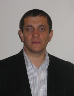 Ionut Radu合作论文数IEEE;SOITEC3Jacob R. Lamb合作论文数2
 Tarun Agarwal合作论文数2Margit Pál合作论文数2Aishwarya Chhatre合作论文数2
 Tarushi Agarwal合作论文数2Martin Rau合作论文数2
 Nicola Marzari合作论文数Cavendish Laboratory, Department of Physics, University of Cambridge;École Polytechnique Fédérale de Lausanne2
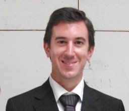 Miguel V Drummond合作论文数2Maurice O'Sullivan合作论文数Ciena Corp2
 George K. Tofaris合作论文数Nuffield Department of Clinical Neurosciences, University of Oxford2
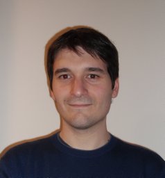 Davide Campi合作论文数Dipartimento di Scienza dei Materiali, Università di Milano-Bicocca2
 Arindam Bhattacharjee合作论文数Sophisticated Analytical Equipment Facility, CSIR-Central Drug Research Institute2
 Kenji Watanabe (渡邊賢司)合作论文数Research Center for Electronic and Optical Materials, National Institute for Materials Science2
 Jain Achint合作论文数2
 Praveen Raghavan合作论文数Apple2
 Nick Doran合作论文数College of Engineering and Physical Sciences, Aston Institute of Photonic Technologies, Aston University2
 Tibor Cinkler合作论文数Dept Telecommun & Media Informat, Budapest Univ Technol & Econ2
 Kim Roberts合作论文数Ciena2M. M. Heyns合作论文数2
 Wim Dehaene合作论文数ESAT-MICAS Laboratory, KU Leuven2




