This paper presents a 7GS/s 8-bit time-interleaved SAR ADC instance produced from a generator-based design flow in a 16nm CMOS FinFET technology. Design techniques such as cross-coupled routing and clock delay modulation are utilized for compatibility with a FinFET process. The time-interleaved SAR ADC layout is automatically generated by placing templates and wires on a grid to abstract design rules. The generated ADC instance with digital calibration achieves 38.2dB SNDR, 97.2fJ/conv-step Walden Figure-of-Merit (FoMW), and 150.6dB Schreier Figure-of-Merit (FoMS), consuming 45.2mW from a 0.95V analog supply and a 0.72V digital supply, and occupying 0.157mm 2 .
This paper demonstrates a signal analysis system-on-chip (SoC) consisting of a general-purpose RISC-V core with vector extensions and a fixed-function signal-processing accelerator. Both the application core and the accelerators are design instances produced through an agile design-space exploration process by generators that allow for a wide range of parameter configurations. The signal processing chain consists of generated instances of a time-interleaved analog-to-digital converter (ADC) followed by a digital tuner, a finite-impulse response (FIR) filter, a polyphase filter, and a fast Fourier transform (FFT) all connected to the five-stage, in-order RISC-V Rocket processor via an AXI4 bus. The generator-based design methodology is detailed, along with the agile design process of producing the fabricated design instance. The 5 mm x 5 mm chip is implemented in a 16-nm FinFET process and operates at 410 MHz at 750 mV drawing 600 mW. Presented applications show coupled functionality of the application processor and accelerator performing spectrometry and radar receive processing, and a comparison with other state-of-the-art application-specific integrated circuits (ASICs) proves that generators can produce performance-competitive designs.
A 1.89-GHz bandwidth, 175-kHz resolution spectral analysis SoC, integrating a subsampling ADC frontend with a digital reconstruction backend and implementing a 21,600-point FFAST sparse FFT [1] has been generated using the Chisel [2] and BAG [3] frameworks in 16-nm CMOS. Three sets of 25×, 27×, and 32×subsampling SAR ADCs acquire signal with ~5.4-6.3 ENOB/slice. The digital backend consists of mixed-radix 864-, 800-, and 675-point FFTs, a signal location estimator, and a peeling decoder that recovers aliased signals from a sparsely populated spectrum. A single-issue, in-order RISC-V Rocket processor interacts with the spectrum analyzer for post-processing and calibration. The ADC consumes 49.8mW with a 3.78-GHz input clock. At 400MHz and 0.7-V VDD, the Rocket core and the FFAST DSP together consume 133.5mW.
Author(s): Wang, Angie | Advisor(s): Nikolic, Borivoje | Abstract: Custom, application-specific implementations of digital signal processing (DSP) systems offer high performance and high energy efficiency, but require significant design and verification effort. Fast Fourier transform (FFT) processors with a broad range of performance requirements are needed for many modern-day signal processing applications, ranging from medical imaging and machine learning to communication and radio astronomy. Certain applications, including modern-day wireless communications, require runtime reconfigurability across a multitude of mixed-radix FFT sizes, high throughput, low latency, and lower power. Convolutional neural networks use multi-dimensional FFTs with stringent requirements on quantization bounds. Despite sharing underlying algorithms and hardware constructs, FFT designs are often difficult to reuse on a per-application or even per-platform basis, leading to redeveloping and reverifying conceptually similar instances. Hardware generators are attractive solutions for effectively balancing fine-grained control of implementation details with simple, rapidly retargetable hardware descriptions, but the existing FFT generators do not support key features like runtime reconfigurability or more general mixed-radix FFTs, limiting their applicability.This thesis presents ACED (A Chisel Environment for DSP), a library extension to the Chisel hardware construction language and the FIRRTL (Flexible Intermediate Representation for RTL) compiler specifically created to simplify the development of hardware DSP generators. ACED allows DSP designs to be specified at a higher level of abstraction, making it easier to add new features as they become necessary. Optimization and specialization are handled via platform-specific compiler passes that promote generator reusability. The ACED library has been used to create a parameterizable memory-based, runtime-reconfigurable 2^n 3^m 5^k 7^l FFT generator to support next-generation wireless systems prototyping. The generator uses a conflict-free, in-place, multi-bank SRAM design, and exploits the duality of decimation-in-frequency and decimation-in-time FFTs to support continuous data flow with ~2N memory. The hardware itself is templated so that Chisel/Scala code can be written to add additional functionality, and users pass parameters to the hardware template via a firmware block. This is the essence of the Chisel DSP generator methodology. The FFT generator has been proven via a 0.37-mm^2 LTE/Wi-Fi compatible FFT RISC-V accelerator instance with measured performance and area comparable to state-of-the-art. To demonstrate the use case of the FFT generator in a larger systems context, a low-power signal acquisition front end capable of sensing frequency-sparse signals in a 1.89-GHz bandwidth with a resolution of 175 kHz in real time has also been prototyped in a 16-nm process. The spectral analysis chip relies on mixed-radix FFTs and reconstruction via the fast Fourier aliasing-based sparse transform (FFAST) algorithm to recover signals in compressed form from a subsampled input. This thesis presents new tools and design methodologies to rapidly design DSP hardware generators---with a particular focus on FFTs---for use in emerging applications such as spectrum sensing for cognitive radio, RADAR, and more.
Designers translate DSP algorithms into application-specific hardware via primitives composed in various ways for different architectural realizations. Despite sharing underlying algorithms and hardware constructs, designs are often difficult to reuse, leading to redeveloping/reverifying conceptually similar instances. Hardware generators are attractive solutions for effectively balancing fine-grained control of implementation details with simple, retargetable hardware descriptions. This work presents ACED, a hardware library for generating DSP systems. It extends the Chisel hardware construction language and FIRRTL compiler and operates on three principles: zero-cost abstraction, unobtrusive downstream optimization/specialization promoting generator reusability, and unified, portable systems modeling and verification.
This paper demonstrates a signal analysis SoC consisting of a general-purpose RISC-V core with vector extensions and a fixed-function signal-processing accelerator. Both the core and the accelerators are instances produced by novel generators that allow for a wide range of parameter configurations and rapid design space exploration. The signal processing chain consists of generated instances of a time-interleaved ADC followed by a digital tuner, FIR filter, polyphase filter, and FFT all connected to the processor via an AXI4 bus. The 5 mm × 5 mm chip is implemented in a 16 nm FinFET process and operates at 410 MHz at 750 mV drawing 600 mW. Presented applications show coupled functionality of the processor and accelerator performing spectrometry and radar receive processing, and a comparison with other state-of-the-art ASICs prove that generators can produce competitive designs.
A single-output, band selecting interposer is designed to combine three identical all-digital CMOS transmitter (Tx) chips. The open-drain CMOS Txs are flip-chip connected to the primary windings of three frequency selecting transformers realized on a single PCB interposer. The secondary windings of the three transformers are connected in series and they share a single output. Across 0.4 to 4 GHz, a peak power higher than 22.9 dBm is achieved collectively by the three sub-Txs with a drain efficiency (DE) better than 25%. The peak powers/DE of the three sub-Txs are 28.6 dBm/50%, 27.4 dBm/49%, and 24.7 dBm/34%, at 0.85, 2.1, and 3 GHz, respectively. This paper further demonstrates that the band selection can be achieved via reconfiguring the CMOS inverse Class-D switching power amplifiers. As demonstrated via continuous wave and 64-quadratic-amplitude modulation, WLAN, and LTE modulation tests, the reconfigurable Tx package exhibits high power and efficiency across all supported bands.
This paper demonstrates a wideband CMOS all-digital polar transmitter with flip-chip connection to three high-density-interconnection PCB interposers. The interposers are designed to extract power from a CMOS open-drain inverse Class-D power amplifier core. For a wide frequency range from 0.7 to 3.5 GHz, continuous-wave output power higher than 25.5 dBm and drain efficiency (DE) above 40% are demonstrated. The low-band package achieves a peak power of 29.2 dBm at 1.1 GHz with DE of 60%, the mid-band package outputs 28.8 dBm at 1.5 GHz with DE of 56%, and the high-band package generates 26 dBm at 3 GHz with DE of 49%. The amplitude modulation (AM) is achieved by digitally modulating the switch conductance of the inverse Class-D core, and the on-chip phase modulation is achieved by digitally weighing the in-phase and quadrature bias currents in the IQ mixer. Detailed modulation tests, involving 64 quadrature amplitude modulation (QAM) and 20-MHz WLAN and LTE signals, exhibit excellent power and efficiency at 0.6, 1.2, 1.8, 2.4, 3, and 3.6 GHz. The associated specifications on spectral masks and error vector magnitudes are satisfied.
A wideband time-division duplex (TDD) front-end with an integrated transmit/receive (T/R) switching technique is implemented in 65nm CMOS. By re-using the PA as an LNA during receive mode, the system eliminates the conventional series T/R switch from the signal path and utilizes only DC mode control switches to enable TDD co-existence. With integrated front-end balun transformer, the full polar transmitter achieves 20dBm peak output power with 32.7% peak drain efficiency. In receive mode, the PA is reconfigured into a wideband 3.4GHz-5.4GHz LNA achieving -6.7dBm P1dB and 5.1dB NF.
Enabled by modern languages and retargetable compilers, software development is in a virtual "Cambrian explosion" driven by a critical mass of powerfully parameterized libraries; but hardware development practices lag far behind. We hypothesize that existing hardware construction languages (HCLs) and novel hardware compiler frameworks (HCFs) can put hardware development on a similar evolutionary path by enabling new hardware libraries to be independent of underlying process technologies including FPGA mappings. We support this claim by (1) evaluating the degree with which Chisel, an existing HCL, can support powerfully parameterized libraries, and (2) introducing the concept and implementation of an HCF that uses an open-source hardware intermediate representation, FIRRTL (Flexible Intermediate Representation for RTL), to transform target-independent RTL into technology-specific RTL. Finally, we evaluate many hardware compiler transformations, including simplifying transformations, analyses, optimizations, instrumentations, and specializations, which demonstrate the power of a combined HCL and HCF approach.
Dedicated hardware accelerators enable energy-efficient implementations of radio and imaging basebands. Multistandard, multi-mode radio basebands require an on-the-fly reconfigurable fast Fourier transform (FFT) accelerator that implements many different FFT sizes. An instance of a runtime-reconfigurable 2 n 3 m 5 k FFT accelerator was generated by a custom hardware generator to meet the requirements of common wireless standards (Wi-Fi, LTE). The accelerator is integrated with a RISC-V processor, and the measured 16nm FinFET chip runs up to 940MHz and consumes 0.46 to 22.6mW of power when running FFT benchmarks for Wi-Fi and LTE symbol lengths.
Runtime-reconfigurable, mixed-radix FFT/IFFT engines are essential for modern wireless communication systems. To comply with varying standards requirements, these engines are customized for each modem. The Chisel hardware construction language has been used in this work to create a generator of runtime-reconfigurable 2(n)3(m)5(k) FFT engines targeting software-defined radios (SDR) for modern communications, but with flexibility to support a wide range of applications. The generator uses a conflict-free, in-place, multi-bank SRAM design, and exploits the duality of decimation-in-frequency (DIF) and decimation-in-time (DIT) FFTs to support continuous data flow with only 2N memory blocks. DFT decomposition using the prime-factor algorithm (PFA) followed by the Cooley-Tukey algorithm (CTA) reduces twiddle ROM sizes. A programmable Winograd's Fourier Transform (WFTA) butterfly supporting radix-2/3/4/5/7 operations reuses radix-7 hardware to support reconfigurability with minimal area penalty. The generated FFTs use 50% less memory than iterative FFTs from Spiral. The twiddle ROM size of the generated LTE/WiFi FFT engine is 16% smaller than that of a 2048-pt Spiral design.
This paper demonstrates a CMOS digital polar transmitter with flip-chip interconnection to low-temperature co-fired ceramic (LTCC) interposers. The LTCC interposers contain the PA output balun targeting different operating frequency bands, and the reconfiguration in the carrier frequency is achieved by selecting an appropriate LTCC interposer. The same CMOS core transmitter is reused for different frequency bands. In this design, an output power higher than 22 dBm from 0.6 to 2.4 GHz is demonstrated, with peak power of 27.1 dBm and peak efficiency of 52%. The polar transmitter includes 9-bit phase interpolation and 8-bit amplitude modulation, suitable and verified as a multi-standard universal digital modulator.
—RAVEN, a state-of-the-art multicore processor being developed by the Berkeley Wireless Research Center, utilizes switched capacitor DC-DC converters to generate dynamically scalable core voltage supplies. It is possible to enhance a core's energy efficiency at a given throughput by allowing the local power management and dedicated clock generator to adapt to the capacitor voltage ripple. Some commercial multicore processors, such as IBM's Power7, support active management of timing guardband to achieve nearly 25% power reduction—without performance degradation—in the face of load-induced supply droops and other noise events similar in characteristic to DC-DC ripple. While previous designs utilized bulky and/or slow-locking DLLs and PLLs for core clock synthesis, our implementation uses a fast-locking, power/area efficient injection-locked ring oscillator. Fast supply adaptation to achieve an average 2GHz core frequency (2x global clock frequency), supported by the aforementioned blocks with feedback from critical path monitors, achieves power savings justifying our scheme for systems needing to tolerate >80mV supply droops.
 Borivoje Nikolic合作论文数Department of Electrical Engineering and Computer Sciences, University of California at Berkeley;Berkeley Wireless Research Center, University of California at Berkeley11
 Elad Alon合作论文数Department of Electrical Engineering and Computer Sciences, University of California, Berkeley;Berkeley Wireless Research Center, University of California, Berkeley9
 Jae-Duk Han合作论文数Sch Elect Elect Engn, Yonsei Univ6
 Jonathan Bachrach合作论文数JITx5
 Zhongkai Wang合作论文数Univ Calif Berkeley, Berkeley, CA 94720 USA4
 Chick Markley合作论文数4
 Bonjern Yang合作论文数4
 Stevo Bailey合作论文数4
 Ali Niknejad合作论文数Electrical Engineering & Computer Sciences, University of California, Berkeley4
 Woorham Bae合作论文数4
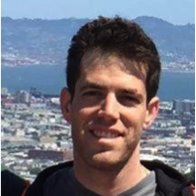 Adam M. Izraelevitz合作论文数Cornell University4
 Paul Rigge合作论文数University of California Berkeley4
 Howard Mao合作论文数Department of Electrical and Computer Engineering, University of California, Davis3
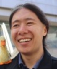 Richard Lin合作论文数University of California, Los Angeles3
 Lingkai Kong (孔令恺)合作论文数Harvard University3
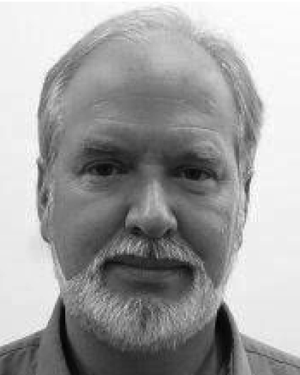 Brian C. Richards合作论文数Department of Electrical Engineering and Computer Sciences, University of California at Berkeley3
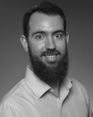 Nathan Narevsky合作论文数3
 Wen Hau Ma合作论文数2
 Mark Snowden合作论文数2
 Joseph Cole合作论文数2Jim McGrath合作论文数2Vason P. Srini合作论文数2
 Sergio Montano合作论文数2Mike Stellfox合作论文数2Franco DeSeta合作论文数2
 Darin Heckendorn合作论文数2
 Akalu Lentiro合作论文数2Steve Shauck合作论文数2Ronen Shoham合作论文数2Justin Norsworthy合作论文数2
 Munir Razzaque合作论文数2
 Matthew Doerflein合作论文数2
 Eric Chang合作论文数Department of Radiology, School of Medicine, University of California, San Diego2
 Charles Wu合作论文数2
 Nai-Chung Kuo合作论文数Broadcom Inc.2
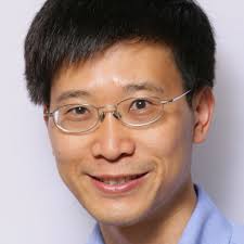 Eric I-Chao Chang (張益肇)合作论文数AI + Health Startups2James Dunn合作论文数1
 Amy Whitcombe合作论文数1
 Pengpeng Lu合作论文数1Jack Koenig合作论文数Univ Calif Berkeley, Dept Elect Engn & Comp Sci, Berkeley, CA 94720 USA1
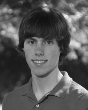 Palmer Dabbelt合作论文数Univ Calif Berkeley, Dept Elect Engn & Comp Sci, Berkeley, CA 94720 USA1Steven Bailey合作论文数1Albert Magyar合作论文数University of California1Chaoying Wu合作论文数1
 Kannan Ramchandran合作论文数Department of Electrical Engineering and Computer Science, University of California, Berkeley1Patrick S. Li合作论文数1
 Dong Gyu Kim合作论文数Department of Neurosurgery, Seoul National University Hospital1
 Colin T. A. Schmidt合作论文数1




