Article de polissage chimico-mecanique pouvant etre une seule couche contigue ayant une surface de polissage, la couche etant une feuille allongee sensiblement rectangulaire ayant une largeur et une longueur au moins quatre fois superieure a la largeur. La fabrication d'un article de polissage peut comprendre les operations consistant a deposer un precurseur liquide sur une courroie transporteuse, durcir au moins en partie le precurseur liquide pendant qu'il est sur la courroie transporteuse pour constituer une couche de polissage et a detacher la couche de polissage de la courroie.
The development of a direct polish process for STI CMP on 200mm wafers using highselectivity slurry (HSS) has been achieved for production of 0.13μm technology microelectronic devices. The new process has improved on-wafer performance compared to standard STI CMP processes. The step height range across the wafer was decreased by 84%, planarity Cpk values (silicon nitride thickness and step-height uniformity) were increased by >25%, leakage current statistics were superior, and the cost of ownership was lowered by 78%. Cross-sectional SEMs both after direct polish CMP and after removal of the silicon nitride show improved planarity.
Wafers where deposited with BPSG films having phosphorus concentration varying from 3.65 to 6.25% and boron concentration varying from 4 to 5.7%. These wafers were polished using CMP and the rates were found to depend on dopant concentrations. A fit to the data indicated that removal rates were more than 3 times as sensitive to boron concentration compared to phosphorus concentration. For a constant phosphorus concentration of 5%, each percent increase in boron increases CMP removal rate by 340 Å/min. For a constant boron concentration of 5%, each percent increase in phosphorus increases CMP removal rate by 96 Å/min.
This paper will review and report significant advances in front end CMP and integration solutions that can be used for future IC devices. In order to increase tool availability and fab operation efficiency, a onetool-for-all-application approach is used. In addition, these methods are compared to the capability of a next generation web tool with slurry-free polishing. The CMP technologies that are required for future generation devices include an advanced polishing head, an advanced in-situ endpoint system, and multiplaten, multi-head architecture. Coupling these hardware elements with next generation consumables, (solo hard pad, high planarity slurry, slurry-free polishing) enables direct polish STI process solutions that meet device requirements for 0.18µm and beyond. Polysilicon CMP is accomplished using a novel multistep process. An advanced PMD process is demonstrated that exhibits a longer life pad and an advanced diamond disk for high throughput and high tool-availability. All the technologies have been successfully used or are currently being tested in production.
A new set of wafer-scale patterns has been designed for analysis and modeling of key CMP effects. In particular, the goal of this work is to develop methods to characterize the planarization capability of a CMP process using simple measurements on wafer scale patterns. We examine means to pattern large trenches (e.g. 1 to 15 mm wide and 15 mm tall) or circles across 4” and 8” wafers, and present oxide polish results using both stacked and solo pads in conventional polish processes. We find that large separation (15 mm) between trenches enables cleaner measurement and analysis. Examination of oxide removal in the center of the trench as a function of trench width shows a saturation at a length comparable to the planarization length extracted from earlier studies of small-scale oxide patterns. Increase in polish pressure is observed to decrease this saturation point. Such wafer scale patterns may provide information on pad flexing limits in addition to planarization length, and promise to be useful in both patterned wafer CMP modeling and studies of wafer scale CMP dependencies such as nanotopography.
 Thomas H. Osterheld合作论文数CMP Division10Anand N. Iyer合作论文数9gopalakrishna b prabhu合作论文数8peter mcreynolds合作论文数7erik s rondum合作论文数7gregory e menk合作论文数7Garlen C. Leung合作论文数6Peter McKeever合作论文数4raymond r jin合作论文数2jeffrey drue david合作论文数2sidney p huey合作论文数2doyle e bennett合作论文数2Deepak Kumar合作论文数2christopher w smith合作论文数2huanbo zhang合作论文数2
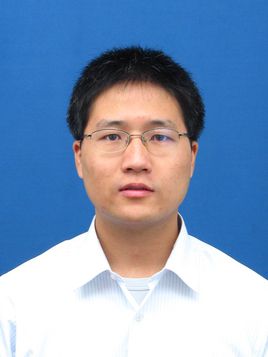 Shijian Li (李石坚)合作论文数College of Computer Science and Technology, Zhejiang University2Wei-Yung Hsu合作论文数2Boris Fishkin合作论文数2christopher heunggyun lee合作论文数1charles c garretson合作论文数1steven m zuniga合作论文数1maurizio tremolada合作论文数1donald kim aun chua合作论文数1antonella martin合作论文数1Brian Lee合作论文数1Terence Gan合作论文数Microsystems Technology Laboratories;Massachusetts Institute of Technology;Taiwan Semiconductor Manufacturing Company;Microsystems Technology Laboratories, Massachusetts Institute of Technology1Sen-Hou Ko合作论文数1
 Duane Boning合作论文数Department of Electrical Engineering & Computer Science, Massachusetts Institute of Technology1Chad Garretson合作论文数1




