An optical detection system that utilizes an electrolumines cent (EL) illumination source is provided. Unlike illumina tion sources used with some conventional optical detection systems, an EL device is relatively homogeneous and diffuse, and thus may provide uniform illumination to the test sample. In addition, the emitted light intensity of the EL device may be easily controlled by simply varying the Voltage or the frequency of the applied current. The relatively flexibility of EL devices may also allow them to be readily incorporated into a chromatographic-based assay device for detecting the presence or absence of an analyte within a test sample.
Unique constraints encountered in the III-N semiconductor system, such as a lack of cleaving planes and resistance to wet etchants, make conventional approaches to the fabrication of laser diodes difficult to implement, and result in the need for novel cavity designs. Improvements in in-plane cavities include etching facets using a focused ion beam and the incorporation of gratings to decrease losses associated with poor mirrors. Towards the fabrication of an electrically pumped VCSEL, the issue of the bottom mirror can be addressed by the use of dielectric mirrors, and either the removal of the sapphire substrate or its incorporation into the cavity by using a curved backside mirror. This paper will review recent developments in these areas at UC Santa Barbara.
Series-connected, two- and three-stage segmented 1.55 µm ridge lasers have been fabricated and are shown to exceed the differential efficiency of comparable control lasers by factors of 1.75 and 2.35. Threshold currents are 1.52 and 2.44 times lower, respectively.
We have fabricated GaN-based light-emitting diodes using transparent indium tin oxide (ITO) p contacts. ITO-contacted devices required an additional 2 V to drive 10 mA, as compared to similar devices with metal contacts. However, ITO has lower optical absorption at 420 nm (α=664 cm−1) than commonly used thin metal films (α=3×105 cm−1). Uniform luminescence was observed in ITO-contacted devices, indicating effective hole injection and current spreading.
Series-connected, two- and three-stage segmented 1.55 /spl mu/m ridge lasers have been fabricated and are shown to exceed the differential efficiency of comparable control lasers by factors of 1.75 and 2.35. Threshold currents are 1.52 and 2.44 times lower, respectively.
1.55 μm ridge lasers were electrically segmented and monolithically driven in series, resulting in 2.35 times higher differential efficiency and 2.44 times lower threshold current in the 3-stage device
A new concept for improving the performance of quantum-well (QW) lasers is reported. The enhancement, both in static and dynamic characteristics, was accomplished by the use of Te n-type delta-doping, coupled to a single strained InGaAs-GaAs QW. The internal parameters were investigated, and their enhancement origin is revealed It is shown to be mainly a consequence of the higher carrier population in the QW and due to the strong coupling between the QW and the delta-doping well.
It is demonstrated that the incorporation of Te n-type δ doping close to a single-strained InGaAs/GaAs quantum well improves the temperature stability of the laser, as indicated by the higher characteristic temperature and by the reduced sensitivity of the threshold current to temperature variations. This improvement results from the strong coupling between the quantum well and the δ-doping well.
Improved dynamic properties of strained single quantum well (QW) lasers were obtained by the incorporation of an n-type δ doping at close proximity to the strained QW active layer. The resultant modulation bandwidth was almost doubled, from 3.5 GHz to more than 6.2 GHz. The increased modulation bandwidth is attributed to an improved carrier injection resulting from the enhancement of the carrier transit time into the QW, as well as a decrease in the significance of the adverse contribution of carrier transport effects.
It is demonstrated that placing an n-type Te δ doping aside a single strained quantum well (QW) is an efficient way to control the initial carrier concentration in the QW and thus to lower transparency current density, Jtr, while preserving low internal losses. This is in contrast with uniform doping of the active area. Jtr of 11.3 A/cm2 and threshold current density of 54.4 A/cm2, which are both the lowest values reported to date for strained InxGa1−xAs/GaAs semiconductor lasers, were obtained. A somewhat higher injection efficiency is obtained when the energy levels are adjusted so that the electrons tunnel from the delta well directly into the QW.
By using a combination of a single strained quantum well with a n-type /spl delta/-doped layer, the transparency current density of the laser was lowered. It was achieved without increasing the internal losses, in contrast with a uniformly doped active area.
Partially relaxed InxGa1−xAs strained-well layers of a fixed thickness above critical, grown on GaAs and capped by GaAs of different thicknesses, were studied by Raman spectroscopy in conjunction with Auger electron spectroscopy and secondary-ion-mass spectroscopy. It is shown that further strain relaxation of the well takes place with increasing GaAs capping thickness initially, but for cap thickness above 100 Å this trend is reversed. This puzzling result is explained by the 3D growth mode. The presence of a high concentration of dislocations intensifies the diffusion of indium to the extent that the two layers become indistinguishable by all three methods. This diffusion of indium is severely reduced with increasing strain.
 Marina Blumin合作论文数8
 Dan Fekete合作论文数California Institute of Technology8
 Larry A. Coldren合作论文数Optoelectronics Technology Center, Department of Electrical & Computer Engineering, College of Engineering, University of California, Santa Barbara5
 Amber Abare合作论文数4T. Margalith合作论文数3
 Gadi Eisenstein合作论文数Russell Berrie Nanotechnology Institute3Getty, J.T.合作论文数3Hansen, M.合作论文数3
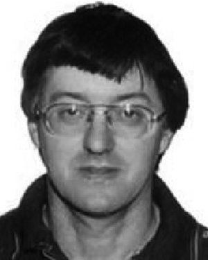 Meir Orenstein合作论文数3
 Randal A. Salvatore合作论文数California Institute of Technology3
 Steven P. Denbaars合作论文数Solid State Lighting & Energy Electronics Center, University of California, Santa Barbara3DA Cohen合作论文数2m yust合作论文数2K.S. Grabowski合作论文数Naval Research Laboratory, Washington, DC 20375, United States2
 I. Samid合作论文数2Rona Sarfaty合作论文数2P. G. Piva合作论文数2
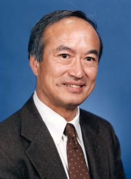 Alfred Y. Cho (卓以和)合作论文数Bell Labs1Hutchinson Albert Lee合作论文数1douglas george james sutherland合作论文数1thomas gordon beck mason合作论文数1Sang-Hun Park合作论文数1m j ries合作论文数1e i chen合作论文数1
 Matthias Richwin合作论文数1yongsoon baek合作论文数1Hisaya Sato合作论文数1
 Dennis Deppe合作论文数University of Central Florida;Sdphotonics, Llc1Gi Stegeman合作论文数1
 Sh Groves合作论文数1Jp Donnelly合作论文数1Dl Ederer合作论文数1joshua s fu合作论文数1y y zhu合作论文数1m joschko合作论文数1
 Daniel A. Cohen合作论文数1michael mack合作论文数luxtera1
 Diana L. Huffaker合作论文数Electrical and Computer Engineering Department, School of Engineering, University of California, Los Angeles1Karl D. Hirschman合作论文数rochester institute of technology1Koontz, E.M.合作论文数1
 Leonid Tsybeskov合作论文数Electrical and Computer Engineering Center, New Jersey Institute of Technology;Department of Electrical and Computer Engineering, New Jersey Institute of Technology1Irith Baumann合作论文数1
 Philippe Fauchet合作论文数School of Engineering, Vanderbilt University1
 Wolfgang Sohler合作论文数Department of Physics, Faculty of Science, University of Paderborn;Department of Applied Physics, Faculty of Science, University of Paderborn1
 Mihail Sigalas合作论文数Department of Materials Science, University of Patras1
 Carlo Sirtori合作论文数Laboratoire de Physique, Ecole Normale Supérieure1Reuven Brener合作论文数Department of Materials Engineering and Solid State Institute, Technion-Israel Institute of Technology1
 Yogesh K. Vohra合作论文数Department of Physics, College of Arts and Sciences, The University of Alabama, Birmingham1
 Gaetano Scamarcio合作论文数Dipartimento di Fisica, Università degli studi di Bari Aldo Moro1




