The AlGaInP/GaP wafer-bonded transparent-substrate (TS) light-emitting diodes (LEDs) have been shown to exhibit luminous efficiencies exceeding many conventional lightning sources including 60 W incandescent sources. This paper will demonstrate the feasibility of scaling wafer bonding technology to 75 mm diameter wafers and some of the unique challenges associated with this scaling. The quality and uniformity of bonding were characterized via scanning acoustic microscopy, white light transmission measurements, full-wafer mapping of parametric performance, and operating life tests. High bonding yields over large areas facilitate low-cost, high-volume fabrication of TS AlGaInP/GaP LEDs, and thus, further enable these devices to compete with other lighting sources.
A truncated-inverted-pyramid (TIP) chip geometry provides substantial improvement in light extraction efficiency over conventional AlGaInP/GaP chips of the same active junction area (∼0.25 mm2). The TIP geometry decreases the mean photon path-length within the crystal, and thus reduces the effects of internal loss mechanisms. By combining this improved device geometry with high-efficiency multiwell active layers, record-level performance for visible-spectrum light-emitting diodes is achieved. Peak efficiencies exceeding 100 lm/W are demonstrated (100 mA dc, 300 K) for orange-emitting (λp∼610 nm) devices, with a peak luminous flux of 60 lumens (350 mA dc, 300 K). In the red wavelength regime (λp∼650 nm), peak external quantum efficiencies of 55% and 60.9% are measured under direct current and pulsed operation, respectively (100 mA, 300 K).
A new form of Al,,Ga,-+s-GaAs-In,Ga, -As quantum well heterostructure (QWH) laser that is confined above and below the active region by an insulating low refractive index native oxide is demonstrated. The laser diodes are defined from a mesa edge by the selective lateral oxidation and anisotropic oxidation of high Al composition Al,,Ga,-,As layers (y=O.85, 0.87) located above and below the QW and waveguide active region. This structure provides excellent current and optical confinement, resulting in continuous wave threshold currents of 8 mA and maximum output powers (uncoated laser) of 35 mW/ facet for a-2.5 pm aperture.
We describe record performance (both external quantum efficiency and luminous efficiency) for cubic-shaped light emitting diodes (LEDs) emitting in the yellow-to-red portion of the visible spectrum. Amber (peak wavelength of 590 nm) and red (630 nm) transparent-substrate (TS) (Al/sub x/Ga/sub 1-x/)/sub 0.5/In/sub 0.5/P/GaP wafer-bonded LEDs are demonstrated with luminous efficiencies exceeding 50 lm/W. These devices exhibit a 1.4/spl times/ improvement over the previous state-of-the-art TS AlGaInP LEDs.
Improvement of 1.4× in the external quantum efficiency and luminous efficiency (lm/W) of transparent-substrate (AlxGa1−x)0.5In0.5P/GaP light-emitting diodes is demonstrated. The improvement is accomplished by reducing the thickness of the active layer to ⩽2000 Å and increasing the internal quantum efficiency by using multiple thin (⩽500 Å) active layers. The maximum luminous efficiency achieved is 73.7 lm/W at λp∼615 nm and the maximum external quantum efficiency is 32.0% at λp∼632 nm.
Data are presented on the photopumped laser operation of planar AlAs–GaAs superlattice (SL) minidisk lasers. The SL minidisk (70 Å AlAs, 30 Å GaAs; 100 periods; ∼37 μm diameter) is defined by impurity-induced layer disordering (IILD), followed by wet oxidation (N2+H2O vapor, 400 °C which surrounds the minidisk with a low-refractive-index AlGaAs oxide. The planar minidisks exhibit laser operation at λ∼7540 Å, with wider mode separation (Δλ∼13 Å) than disks defined by only IILD (a smaller refractive index step) and cleaved sample edges. The mode separation of Δλ∼13 Å corresponds to disk modes that utilize the perimeter of the oxide-defined disks. In the fabrication of the SL minidisks, IILD forms a structural and doping difference beyond the disk perimeter that acts, in effect, as a p–n junction during etching or wet oxidation. Etch profiles are shown demonstrating this behavior.
Data are presented demonstrating the effect that cavity length, and thus Q, has upon quantum well heterostructure edge-emitting laser diodes that are reduced to microcavity thickness. The lasers, with reduced mode density and enhanced spontaneous emission, are defined vertically by a Ag top-contact mirror and a closely spaced (∼0.9 μm) high-contrast AlAs native oxide-GaAs distributed Bragg reflecting bottom mirror. For shorter and shorter diode lengths (700→70 μm, and still lesser mode density) the light versus current (L–I) characteristic below threshold is at first steeper and steeper (amplified stimulated emission), until, at a diode length of ∼100 μm, the loss in Q and insufficient gain are manifest as a downward bend in the L–I curve and a shift to higher threshold current where bandfilling to a higher state (shorter wavelength) contributes more gain.
Data are presented demonstrating photopumped laser operation of a planar photonic lattice (∼1 μm thick) that is comprised of 9 μm disks with 2 μm separation arranged in a two-dimensional hexagonal close-packed pattern. The active region of each disk is an AlAs (70 Å)–GaAs (30 Å) superlattice (100 periods). The disks are defined by impurity-induced layer disordering, followed by wet oxidation (N2+H2O vapor, 400 °C), which surrounds each disk with a low-refractive-index AlGaAs native oxide. The photonic lattice exhibits laser operation within wide (Δλ∼17 Å) spectral bands that are spaced according to the disk modes, and that propagate light anisotropically in the plane of the lattice. In addition to the extended lattice, groups of seven disks are studied and are seen to display similar behavior.
Data are presented on the 300 K photopumped (pulsed) laser operation of ultrathin (∼0.15 μm) planar microdisk lasers. The tiny lasers employ the wet oxidation of an AlGaAs layer beneath the disks to form semiconductor cavities that are in solid contact but optically isolated from the GaAs substrate. The resulting microcavity lasers operate at low pump intensities and exhibit spectra characteristic of whispering gallery mode microdisk lasers.
Data are presented demonstrating double injection and negative resistance in stripe-geometry oxide-aperture AlyGa1−yAs–GaAs–InxGa1−xAs quantum well heterostructure lasers. The buried oxide laser structures are defined, in current and cavity, by laterally oxidizing the higher Al composition upper and lower cladding layers from a mesa edge (a ridge), thus, forming a narrow oxide-defined buried aperture (∼2μm). Post fabrication annealing (425 °C in N2) removes the negative resistance, indicating that the crystal growth and oxidation processes introduce products such as H and OH in the active region that compensate the dopants.
At atmospheric conditions high Al Composition Al{sub x}Ga{sub 1-x}As (x {ge}0.7) in Al{sub x}Ga{sub 1-x}As-GaAs heterostructures is subject to failure via hydrolyzation. In contrast, {open_quotes}wet{close_quotes} oxidation at higher temperatures ({ge}400{degrees}C) produces stable AlGaAs native oxides that prove to be useful in quantum well heterostructure devices. The {open_quotes}wet{close_quotes} oxidation process results in the conversion of high Al composition heterostructure material into a stable low refractive index, current-blocking native oxide, which can be used to define cavities and current paths. The oxidation can be used to passivate exposed Al-bearing surfaces. Its selective, anisotropic nature is also useful for the fabrication of both planar and non-planar devices, including buried-oxide heterostructures. The III-V native oxide has been used in the fabrication of single-stripe and stripe array lasers, ring lasers, coupled-cavity lasers, buried-oxide verticle cavity lasers, deep-oxide waveguides, deep-oxide lasers, and high reliability LED`s. Also, the native oxide of A1As has been demonstrated in field effect transistor operation. The use of the III-V native oxide in various device applications is described.
Data are presented on the 300 K photopumped (pulsed) laser operation of a visible-spectrum (λ=650 nm) AlAs–AlGaAs/InAlP–InGaP quantum-well heterostructure (QWH) crystal that utilizes high-index-contrast AlAs-native-oxide/Al0.6Ga0.4As distributed Bragg reflector mirrors. The mirrors are formed by the lateral oxidation (H2O+N2, 425 °C) of two sets of four ‘‘buried’’ AlAs layers that are separated by Al0.6Ga0.4As. These mirrors, which create a high-Q cavity in the vertical direction, ‘‘sandwich’’ a one-wavelength InAlP–InGaP QW active region, thus forming a compact microcavity that ‘‘tunes’’ the carrier scattering and recombination into a narrow spectrum (∼25 Å) and supports laser operation in the vertical direction.
Data are presented demonstrating edge-emitting laser diode operation of AlyGa1−yAs– GaAs–InxGa1−xAs quantum well heterostructures modified by the formation of a buried native-oxide distributed Bragg reflecting (DBR) mirror adding vertical confinement to the longitudinal laser cavity. The bottom DBR mirror, combined with the highly reflective top p-contact metallization (Ag), forms a thin broadband vertical cavity. The auxiliary vertical mirrors are tuned to improve the coupling of the spontaneous emission to the longitudinal lasing mode, resulting in reduced threshold currents and modified emission characteristics below threshold.
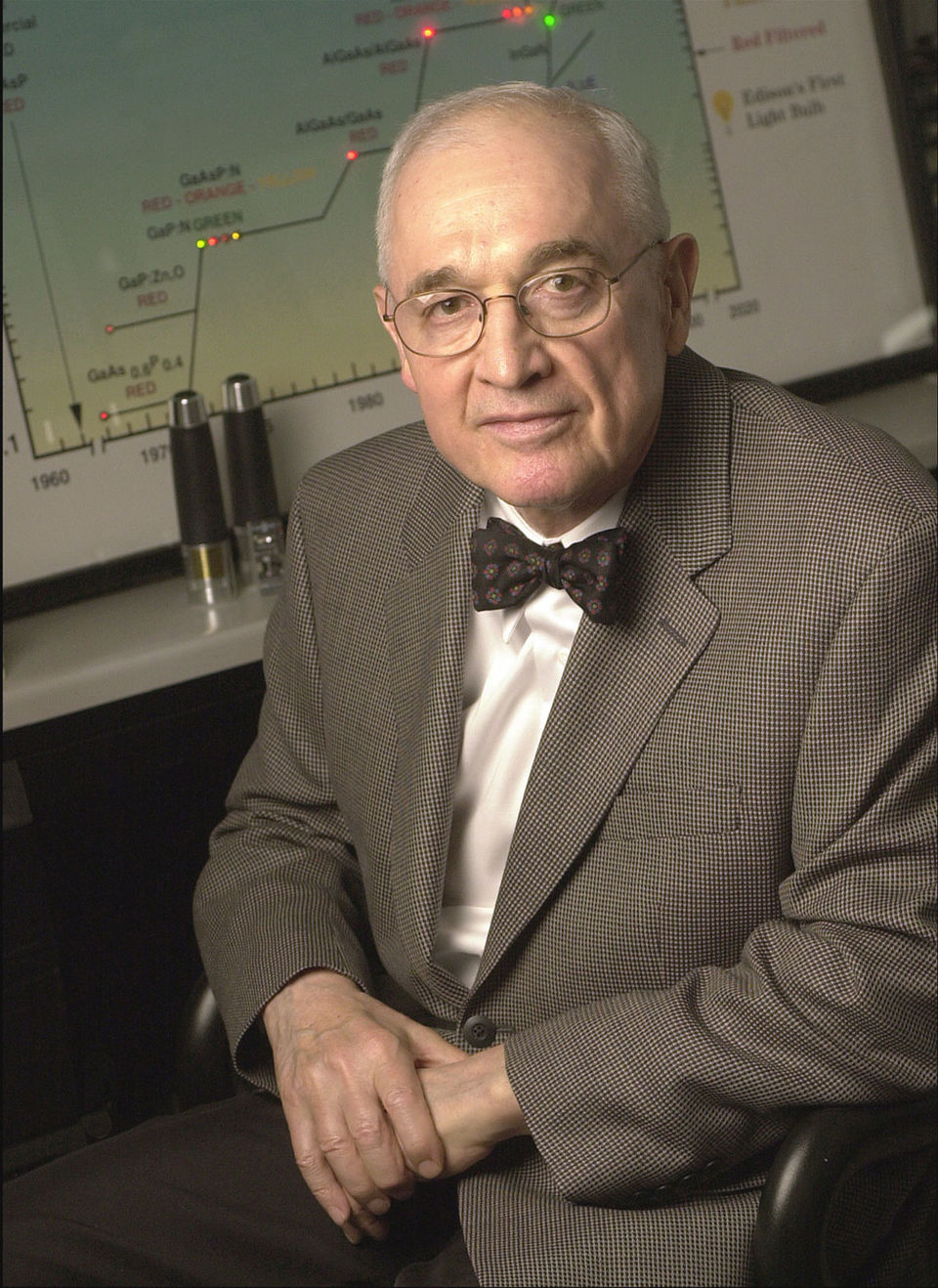 Nick Holonyak合作论文数Holonyak Micro & Nanotechnology Lab, The Grainger College of Engineering, University of Illinois at Urbana-Champaign24
 S. A. Maranowski合作论文数12m j ries合作论文数11
 Mike Krames合作论文数Arkesso LLC;Opnovix Corp.9
 Tryphone Richard合作论文数8Alan R. Sugg合作论文数8
 Fred Kish合作论文数Department of Electrical and Computer Engineering, North Carolina State University;Monteith Research Center, North Carolina State University6
 Nathan Gardner合作论文数LumiLeds Lighting6h c chui合作论文数5Sa Stockman合作论文数5JW Huang合作论文数5Patrick Nolan Grillot合作论文数5Christopher Kocot合作论文数Finisar Corporation4
 Kuo-Cheng Hsieh合作论文数4G. Höfler合作论文数4p w evans合作论文数3a d minervini合作论文数3ih tan合作论文数3J.E. Baker合作论文数3
 Russell Dean Dupuis合作论文数School of Electrical and Computer Engineering, College of Engineering, Georgia Institute of Technology3c cartercoman合作论文数2Ts Tan合作论文数2Cp Kocot合作论文数2Islam, M.R.合作论文数2
 S.C. Tan (陳秀聰)合作论文数Department of Electrical and Electronic Engineering, University of Hong Kong2J. Posselt合作论文数2Mark R Hueschen合作论文数2Bk Loh合作论文数2
 Archie L. Holmes Jr.合作论文数Chandra Department of Electrical and Computer Engineering, Cockrell School of Engineering, University of Texas at Austin2Gail Sasser合作论文数2
 M. George Craford合作论文数Philips Lumileds Lighting Company2Steve A. Stockman合作论文数2N Finnegan合作论文数2D Collins合作论文数1douglas george james sutherland合作论文数1yinglan chang合作论文数1yongsoon baek合作论文数1Gi Stegeman合作论文数1
 Sh Groves合作论文数1Jp Donnelly合作论文数1Dl Ederer合作论文数1A. FL Sugg合作论文数1m yust合作论文数1Irith Baumann合作论文数1Buchinsky, O.合作论文数1
 Marina Blumin合作论文数1
 Wolfgang Sohler合作论文数Department of Physics, Faculty of Science, University of Paderborn;Department of Applied Physics, Faculty of Science, University of Paderborn1
 Yogesh K. Vohra合作论文数Department of Physics, College of Arts and Sciences, The University of Alabama, Birmingham1Paul R Elliker合作论文数1




