Metallic rugate filters are theoretically investigated for the first time. Our model builds on randomly dispersed metallic nanorod arrays with sinusoidally varying porosities along the film thickness. It was found that metallic rugate filters can display strong optical response in the visible and near-infrared regions for both TE and TM polarizations and for a wide range of incident angles. Moreover, the optical features of a metallic rugate filter can be fine tuned by adjusting its structural features. Interestingly, multiple-peak rugate filters can be conveniently achieved by combining different periodicities in one rugate structure. The interesting optical behaviors of the novel metal-based reflectors, combined with the many desirable properties of metals (e.g. electric, thermal, magnetic, mechanical, and chemical properties) are bound to lead to various multi-functional optical devices.
Three-dimensional (3D) chip integration with through-silicon-vias (TSV's) can enable system benefits of enhanced performance, power efficiency, and cost reduction leveraging micro-architecture designs such as 2.5D silicon packages and 3D die stacks. 2.5D silicon packages and 3D die stacks structures integrated in modules each have unique technical challenges but each can provide system benefits including lower latency and higher bandwidth compared to traditional packaging solutions. Additional system benefits using 2.5D or 3D integration can include product miniaturization or increased function in the same size product. Leveraging proper design and micro-architecture for a system application, 3D technology can aide chip manufacturability for lower costs, sub-component heterogeneous integration, modular design and sub-component design reuse, which can reduce development expense and decrease time to market. 2.5D and 3D technology can reduce interconnection length between circuits leading to lower power consumption and lower latency as well as increase the number of interconnections which supports increased bandwidth to traditional 2D off chip interconnection. Appropriate design ground rules, clocking, and electrical models should match well defined technology attributes such as TSV's and silicon to silicon interconnection electrical parametrics. In addition a wafer test methodology for known good die (KGD) and high yield assembly integration approach are important to obtain integrated 2.5D and 3D modules. For complex 3D integration, proper consideration for module or integrated die stacked with TSV's and Si to Si interconnection may require redundancy and an integral repair methodology. 2.5D and 3D technology challenges may include an increase in the power delivery and cooling requirements to meet the increased circuit density and power density of these structures. For small, low power applications such as mobile devices, 2.5D and 3D technology can provide substantial benefit through both performance benefit and power savings and lead to longer battery life for the same function. For some high performance and high power applications, the 2.5D approach simplifies heterogeneous die integration without requiring leading to increases power density and heat removal cooling density. Whereas some high performance and high power applications using 3D technology may require extensive planning for power delivery with localized power regulation and specialized cooling approaches to avoid excessive in die stack temperatures while taking advantage of performance gains that these short links between heterogeneous die can provide. 3D die stacks using multi-core processors and wide I/O DRAM, eDRAM, SRAM or cache stacks can provide high bandwidth, performance improvements with lower latency. In addition to the power delivery and thermal challenges of 2.5D and 3D described above, there are 3D fabrication and industry compatibility challenges. Technology challenges include wafer integration and finishing with TSV's, test for known-good-die (KGD), assembly and module integration. Infrastructure compatibility and use of newly evolving industry standards such as Semi-3D standards for wafer handling and JEDEC standards for wide I/O memory to name two examples. Standards for wafer shipping are underway and other 3D compatibility standards are being defined over time. This research paper describes key challenges to enable systems using 2.5D and 3D technology. The paper also highlights progress and results for 2.5D and 3D hardware demonstrations and gives an outlook on future demonstrations.
The results of stress tests on 50 μm-pitch Pb-free microbump interconnect 3D Si structures are summarized. It was found that thermal processes alone compete strongly with electromigration at stress currents of 50 and 100 mA. Typical test sites exhibited a gradual increase in relative resistance increase over time. While large changes in bump interconnection resistance did occur for some sites, the interconnections were resistant to full open electrical failure, even after subjected to mechanical shock following long-term EM stress. Underfilled samples were more robust than non-underfilled samples. Overall, the results suggest that for application in 3D Si stacks, microbumps can support higher power densities than those used currently with standard pitch bump interconnections.
 P. S. Andry合作论文数45
 John U Knickerbocker合作论文数Cognitive IoT for Heathcare, IBM Research/Diagnostics and Sensing Devices Team, IBM Research/Micro-System Technology & Solutions Team, Thomas J. Watson Research Center, IBM Research38
 Bing Dang合作论文数24
 Raymond R Horton合作论文数17
 Edmund J. Sprogis合作论文数17
 Polastre, R.合作论文数16Steven L. Wright合作论文数15Cs Patel合作论文数10Bucknell C. Webb合作论文数10chirag s patel合作论文数9K. Sakuma合作论文数8e sprogis合作论文数8
 Fuad E. Doany合作论文数Thomas J. Watson Research Center, IBM Research8L. P. Buchwalter合作论文数7
 Christian Baks合作论文数7
 Young-Je Kwark合作论文数Department of Organic Materials and Fiber Engineering, Soongsil University7
 Christian Schuster合作论文数Institut für Theoretische Elektrotechnik, School of Electrical Engineering, Computer Science, and Mathematics, Hamburg University of Technology;Lothar Collatz Center for Computing in Science, University of Hamburg6Sprogis, E.J.合作论文数6
 Clint Schow合作论文数Department of Electrical and Computer Engineering, College of Engineering, University of California Santa Barbara6
 Anna W. Topol合作论文数IBM T.J. Watson Research Center6Jeffrey A. Kash合作论文数Center for Integrated Science and Engineering, Columbia University6bucknell c webb合作论文数5John M. Cotte合作论文数5
 Kuan-Neng Chen (陳冠能)合作论文数3DIC Lab, Institute of Electronics, National Chiao Tung University;Institute of Innovative Research, Tokyo Institute of Technology;Industrial Technology and Research Institute5j rosner合作论文数4A. Sharma合作论文数4russell alan budd合作论文数3H Nyikal合作论文数3richard p volant合作论文数3
 bruce k furman合作论文数3
 Benjamin G. Lee合作论文数NVIDIA3
 Keith A. Jenkins合作论文数IBM Thomas J. Watson Research Center3Gerard Mcvicker合作论文数3
 Kuniaki Sueoka合作论文数3
 Lavanya Turlapati合作论文数3
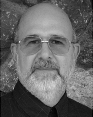 Robert Trzcinski合作论文数3Edward C Cooney合作论文数3
 Roger Dangel合作论文数3Frank Libsch合作论文数Sherman Fairchild Center, Lehigh University3
 Sri M. Srijayantha合作论文数3David L Rath合作论文数3
 Evan G Colgan合作论文数Thomas J. Watson Research Center3
 Timothy O. Dickson合作论文数Dept ., ECE;University of Toronto;ECE Dept ., University of Toronto3
 Daniel M. Kuchta合作论文数IBM T. J. Watson Research Center3Yukifumi Oyama合作论文数3
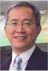 Edwin Y. B. Pun合作论文数Department of Electronic Engineering, City University of Hong Kong3John Magerlein合作论文数3PATEL C合作论文数2p chiniwalla合作论文数2




