Spins associated to solid-state color centers are a promising platform for investigating quantum computation and quantum networks. Recent experiments have demonstrated multiqubit quantum processors, optical interconnects, and basic quantum error-correction protocols. One of the key open challenges towards larger-scale systems is to realize high-fidelity universal quantum gates. In this work, we design and demonstrate a complete high-fidelity gate set for the two-qubit system formed by the electron and nuclear spin of a nitrogen-vacancy center in diamond. We use gate set tomography (GST) to systematically optimize the gates and demonstrate single-qubit gate fidelities of up to 99.999(1)% and a two-qubit gate fidelity of 99.93(5)%. Our gates are designed to decouple unwanted interactions and can be extended to other electron-nuclear spin systems. The high fidelities demonstrated provide opportunities towards larger-scale quantum processing with color-center qubits.
Nitrogen vacancy centres in diamond can be used for vector magnetometry. In this work we present a portable vector diamond magnetometer. Its vector capability, combined with feedback control and robust structure enables operation on moving platforms. While placed on a trolley, magnetic mapping of a room is demonstrated and the magnetometer is also shown to be operational in a moving van with the measured magnetic field shifts for the x, y, and z axes being tagged with GPS coordinates. These magnetic field measurements are in agreement with measurements taken simultaneously with a fluxgate magnetometer.
The decoherence of a central electron spin due to the dynamics of a coupled electron-spin bath is a core problem in solid-state spin physics. Ensemble experiments have studied the central spin coherence in detail, but such experiments average out the underlying quantum dynamics of the bath. Here, we show the coherent back-action of an individual NV center on an electron-spin bath and use it to detect, prepare and control the dynamics of a pair of bath spins. We image the NV-pair system with sub-nanometer resolution and reveal a long dephasing time (T_2^* = 44(9) ms) for a qubit encoded in the electron-spin pair. Our experiment reveals the microscopic quantum dynamics that underlie the central spin decoherence and provides new opportunities for controlling and sensing interacting spin systems.
Vector magnetometry provides more information than scalar measurements for magnetic surveys utilized in space, defense, medical, geological and industrial applications. These areas would benefit from a mobile vector magnetometer that can operate in extreme conditions. Here we present a scanning fiber-coupled nitrogen vacancy (NV) center vector magnetometer. Feedback control of the microwave excitation frequency is employed to improve dynamic range and maintain sensitivity during movement of the sensor head. Tracking of the excitation frequency shifts for all four orientations of the NV center allow us to image the vector magnetic field of a damaged steel plate. We calculate the magnetic tensor gradiometry images in real time, and they allow us to detect smaller damage than is possible with vector or scalar imaging.
Spins associated to optically accessible solid-state defects have emerged as a versatile platform for exploring quantum simulation, quantum sensing and quantum communication. Pioneering experiments have shown the sensing, imaging, and control of multiple nuclear spins surrounding a single electron spin defect. However, the accessible size of these spin networks has been constrained by the spectral resolution of current methods. Here, we map a network of 50 coupled spins through high-resolution correlated sensing schemes, using a single nitrogen-vacancy center in diamond. We develop concatenated double-resonance sequences that identify spin-chains through the network. These chains reveal the characteristic spin frequencies and their interconnections with high spectral resolution, and can be fused together to map out the network. Our results provide new opportunities for quantum simulations by increasing the number of available spin qubits. Additionally, our methods might find applications in nano-scale imaging of complex spin systems external to the host crystal.
NV-based magnetometry in single-crystal diamond grown by chemical vapour deposition (CVD), is now a wellestablished technology with demonstrated applications in DC and AC bulk magnetometry. The approx. 500 µm thick plates normally used offer limited contrast when attempting to measure the magnetic properties of small samples (for example biological samples or minerals) placed in proximity of the diamond magnetic sensor. Such applications would benefit from a few µm high-[NV] layer on a low luminescence substrate in order to collect the signal only from NV centres spatially close to the area of interest, allowing the formation of a magnetic image with increased resolution. It is important to ensure that the strain in the high-[NV] layer is spatially uniform and low in magnitude, to preserve the magnetic resolution and to avoid unusable regions on the magnetic sensor. Established techniques to manage strain during CVD diamond growth are not applicable for the deposition of a few µm of material; normally, the substrate would undergo extensive plasma etching to remove contaminants and polishing damage from the surface of the substrate. This is not possible for thin layers, since the etching would increase the roughness and produce NV layers with non-uniform thickness. Here, we present recent developments to obtain thin, high-[NV] layers on high purity substrates with large areas of low strain, by discussing the substrate preparation and strain characterisation before and after growth.
Ensembles of nitrogen vacancy centres (NVCs) in diamond can be employed for sensitive magnetometry. In this work we present a fiber-coupled NVC magnetometer with an unshielded sensitivity of (30 $\pm$ 10) pT/$\sqrt{\textrm{Hz}}$ in a (10 - 500)-Hz frequency range. This sensitivity is enabled by a relatively high green-to-red photon conversion efficiency, the use of a [100] bias field alignment, microwave and lock-in amplifier (LIA) parameter optimisation, as well as a balanced hyperfine excitation scheme. Furthermore, a silicon carbide (SiC) heat spreader is used for microwave delivery, alongside low-strain $^{12}\textrm{C}$ diamonds, one of which is placed in a second magnetically insensitive fluorescence collecting sensor head for common-mode noise cancellation. The magnetometer is capable of detecting signals from sources such as a vacuum pump up to 2 m away, with some orientation dependence but no complete dead zones, demonstrating its potential for use in remote sensing applications.
The negatively charged nitrogen-vacancy centre (NV$^-$) in diamond has been utilized in a wide variety of sensing applications. The centre's long spin coherence and relaxation times ($T_2^*$, $T_2$ and $T_1$) at room temperature are crucial to this, as they often limit sensitivity. Using NV$^-$ centres in nanodiamonds allows for operations in environments inaccessible to bulk diamond, such as intracellular sensing. We report long spin coherence and relaxation times at room temperature for single NV$^-$ centres in isotopically-purified polycrystalline ball-milled nanodiamonds. Using a spin-locking pulse sequence, we observe spin coherence times, $T_2$, up 786 $\pm$ 200 $\mu$s. We also measure $T_2^*$ times up to 2.06 $\pm$ 0.24 $\mu$s and $T_1$ times up to 4.32 $\pm$ 0.60 ms. Scanning electron microscopy and atomic force microscopy measurements show that the diamond containing the NV$^{-}$ centre with the longest $T_1$ time is smaller than 100 nm. EPR measurements give an N$_{s}$$^{0}$ concentration of 0.15 $\pm$ 0.02 ppm for the nanodiamond sample.
An improved analysis of the interfacial toughness using nanoindentation induced blistering of thin films on stiff substrates is demonstrated on GaN-on-diamond. The Hutchinson-Suo analysis requires accurate measurement of blister dimensions, conventionally measured using 2-D line-scans from 3-D topographical maps. The new meteorology overcomes shortcomings of this technique by fitting the 3-D analytical solution of a clamped Kicrchoff plate to the topological map of the blister. This allowed for quantification of interfacial toughness of smaller blisters in GaN-on-diamond, previously assumed invalid for analysis due to inadequacies of the line-scan analysis. Three samples were investigated and found to have interfacial toughness ranging from 0.6-1 J m(-2). Additionally, the relationship between residual stress in the GaN and interfacial toughness was investigated using photoluminescence spectroscopy. In all cases, the GaN was found to be under increased compression at the diamond interface by up to-0.81 GPa, although no correlation with interfacial toughness was observed. (C) 2021 Acta Materialia Inc. Published by Elsevier Ltd. All rights reserved.
Quantum networks can enable quantum communication and modular quantum computation. A powerful approach is to use multi-qubit nodes that provide quantum memory and computational power. Nuclear spins associated with defects in diamond are promising qubits for this role. However, dephasing during optical entanglement distribution hinders scaling to larger systems. Here, we show that a 13 C-spin quantum memory in isotopically engineered diamond is robust to the optical link operation of a nitrogen-vacancy centre. The memory lifetime is improved by two orders-of-magnitude upon the state-of-the-art, surpassing reported times for entanglement distribution. Additionally, we demonstrate that the nuclear-spin state can survive ionisation and recapture of the nitrogen-vacancy electron. Finally, we use simulations to show that combining this memory with previously demonstrated entanglement links and gates can enable key network primitives, such as deterministic non-local two-qubit gates, paving the way for test-bed quantum networks capable of investigating complex algorithms and error correction.
Solid-state spin qubits is a promising platform for quantum computation and quantum networks1,2. Recent experiments have demonstrated high-quality control over multi-qubit systems3-8, elementary quantum algorithms8-11 and non-fault-tolerant error correction12-14. Large-scale systems will require using error-corrected logical qubits that are operated fault tolerantly, so that reliable computation becomes possible despite noisy operations15-18. Overcoming imperfections in this way remains an important outstanding challenge for quantum science15,19-27. Here, we demonstrate fault-tolerant operations on a logical qubit using spin qubits in diamond. Our approach is based on the five-qubit code with a recently discovered flag protocol that enables fault tolerance using a total of seven qubits28-30. We encode the logical qubit using a new protocol based on repeated multi-qubit measurements and show that it outperforms non-fault-tolerant encoding schemes. We then fault-tolerantly manipulate the logical qubit through a complete set of single-qubit Clifford gates. Finally, we demonstrate flagged stabilizer measurements with real-time processing of the outcomes. Such measurements are a primitive for fault-tolerant quantum error correction. Although future improvements in fidelity and the number of qubits will be required to suppress logical error rates below the physical error rates, our realization of fault-tolerant protocols on the logical-qubit level is a key step towards quantum information processing based on solid-state spins.
Understanding and protecting the coherence of individual quantum systems is a central challenge in quantum science and technology. Over the past decades, a rich variety of methods to extend coherence have been developed. A complementary approach is to look for naturally occurring systems that are inherently protected against decoherence. Here, we show that pairs of identical nuclear spins in solids form intrinsically long-lived qubits. We study three carbon-13 pairs in diamond and realize high-fidelity measurements of their quantum states using a single nitrogen-vacancy center in their vicinity. We then reveal that the spin pairs are robust to external perturbations due to a combination of three phenomena: a decoherence-free subspace, a clock transition, and a variant on motional narrowing. The resulting inhomogeneous dephasing time is T-2* = 1.9(3) min, the longest reported for individually controlled qubits. Finally, we develop complete control and realize an entangled state between two spin pairs through projective parity measurements. These long-lived qubits are abundantly present in diamond and other solids and provide new opportunities for ancilla-enhanced quantum sensing and for robust memory qubits for quantum networks.
Ensembles of nitrogen-vacancy (NV) centres in diamond are a leading platform for practical quantum sensors. Reproducible and scalable fabrication of NV-ensembles with desired properties is crucial, as is an understanding of how those properties influence performance. This work addresses these issues by characterising nitrogen-doped diamond produced by the chemical vapour deposition (CVD) method across a range of synthesis conditions. This is shown to produce material with widely differing absorption characteristics, which is linked to the level of parasitic defects other than substitutional nitrogen (NS) and NV. In such material, the achievable concentration of NV- ([NV-]) is found to be influenced by the as-grown properties. At the 10-20 ppm level for [NS], the production of CVD-grown material with strain levels sufficient not to limit achievable device sensitivity is demonstrated and a favourable product of [NV-] and T2* is obtained. Additionally, reproducible properties over a batch of 23 samples from a single synthesis run are achieved, which appears promising for the scalability efforts underway in this area of research.
Conventional wisdom holds that macroscopic classical phenomena naturally emerge from microscopic quantum laws 1 – 7 . However, despite this mantra, building direct connections between these two descriptions has remained an enduring scientific challenge. In particular, it is difficult to quantitatively predict the emergent ‘classical’ properties of a system (for example, diffusivity, viscosity and compressibility) from a generic microscopic quantum Hamiltonian 7 – 14 . Here we introduce a hybrid solid-state spin platform, where the underlying disordered, dipolar quantum Hamiltonian gives rise to the emergence of unconventional spin diffusion at nanometre length scales. In particular, the combination of positional disorder and on-site random fields leads to diffusive dynamics that are Fickian yet non-Gaussian 15 – 20 . Finally, by tuning the underlying parameters within the spin Hamiltonian via a combination of static and driven fields, we demonstrate direct control over the emergent spin diffusion coefficient. Our work enables the investigation of hydrodynamics in many-body quantum spin systems.
19th IEEE InterSociety Conference on Thermal and Thermomechanical Phenomena in Electronic Systems Welcome to ITherm 2020 ................................................................................................................................ iii Virtual Program for 2020 ................................................................................................................................ iv ITherm Committees ........................................................................................................................................ vi Keynotes ........................................................................................................................................................... ix ITherm Award of Excellence: “Advanced uElectroncs Packaging Drives Heterogeneous Integration” ...... xi Student Heat Sink Challenge ........................................................................................................................ xii Technology-Talk Sessions ........................................................................................................................... xiii IEEE Heterogeneous Integration Roadmap Workshop ............................................................................. xiv ECTC/ITherm Joint Diversity Panel; Student Poster Session ................................................................... xv ITherm Best Papers from 2019 .................................................................................................................... xvi Call for Papers: ITherm 2021 in San Diego, CA USA .............................................................................. xviii
Understanding and protecting the coherence of individual quantum systems is a central challenge in quantum science and technology. Over the last decades, a rich variety of methods to extend coherence have been developed. A complementary approach is to look for naturally occurring systems that are inherently protected against decoherence. Here, we show that pairs of identical nuclear spins in solids form intrinsically long-lived quantum systems. We study three carbon-13 pairs in diamond and realize high-fidelity measurements of their quantum states using a single NV center in their vicinity. We then reveal that the spin pairs are robust to external perturbations due to a unique combination of three phenomena: a clock transition, a decoherence-free subspace, and a variant on motional narrowing. The resulting inhomogeneous dephasing time is $T_2^* = 1.9(3)$ minutes, the longest reported for individually controlled qubits. Finally, we develop complete control and realize an entangled state between two spin-pair qubits through projective parity measurements. These long-lived qubits are abundantly present in diamond and other solids, and provide new opportunities for quantum sensing, quantum information processing, and quantum networks.
We report the application of phasor analysis and nonlinear iterative fitting to complex spatial and spectroscopic luminescence decay data obtained from multidimensional microscopy of a CVD diamond grown on a HPHT substrate. This spectral and lifetime-resolved analysis enabled spatial mapping of variations in concentrations of nitrogen vacancy (NV) defects in both charge states and the quenching of NV- defects, as well as the identification of SiV- luminescence. These imaging and spectroscopic modalities may be important for reliable fabrication of quantum devices based on such defects in diamond, which will require well-defined and characterised quantum electronic properties.
A promising approach for multi-qubit quantum registers is to use optically addressable spins to control multiple dark electron-spin defects in the environment. While recent experiments have observed signatures of coherent interactions with such dark spins, it is an open challenge to realize the individual control required for quantum information processing. Here, we demonstrate the heralded initialisation, control and entanglement of individual dark spins associated to multiple P1 centers, which are part of a spin bath surrounding a nitrogen-vacancy center in diamond. We realize projective measurements to prepare the multiple degrees of freedom of P1 centers—their Jahn-Teller axis, nuclear spin and charge state—and exploit these to selectively access multiple P1s in the bath. We develop control and single-shot readout of the nuclear and electron spin, and use this to demonstrate an entangled state of two P1 centers. These results provide a proof-of-principle towards using dark electron-nuclear spin defects as qubits for quantum sensing, computation and networks.
Some of the most exciting recent advancements in heat conduction physics have been motivated, enabled, or achieved by the thermal management community that ITherm serves so effectively. In this talk we highlight the resulting renaissance in basic heat conduction research, which is linked to cooling challenges from power transistors to portables. Examples include phonon transport and scattering in nanotransistors, engineered high-conductivity composites, modulated conductivity through phase transitions, as well as the surprising transport properties of low-dimensional (1D and 2D) nanomaterials. This work benefits strongly from decades of collaboration and leadership from the semiconductor industry. Dr. Kenneth E. Goodson chairs the Mechanical Engineering Department, and holds the Davies Family Provostial Professorship and a courtesy appointment in Materials Science at Stanford University. His lab has graduated 40 PhDs, nearly half of whom are professors at schools including MIT, Stanford, and UC Berkeley. Honors include the Kraus Medal, the Heat Transfer Memorial Award, the AIChE Kern Award, the SRC Technical Excellence Award, the InterPACK Achievement Award, and Fellow grade with ASME, IEEE, APS, and AAAS. Goodson co-founded Cooligy, which built computer heat sinks and was acquired by Emerson in 2006. At Stanford, serving as Mechanical Engineering Chair and Vice Chair since 2008, Goodson led two strategic plans and launched hiring of 15 faculty members who are transforming the department’s scholarship and diversity. ITherm 2018, May 29 June 1, 2018 Sheraton Hotel & Marina, San Diego, CA, USA 17 Final Conference Program CONFERENCE KEYNOTES Ravi Kuppuswamy Sean Ross Paolo Petagna Intel ARFL CERN K-1: FPGAS: THE ACCELERATOR OF CHOICE FROM THE EDGE TO THE CLOUD Presenter: Ravi Kuppuswamy (Intel) Wednesday, May 30, 9:00-10:00 AM, Bel Aire Abstract: The computing landscape is dynamically evolving and changing on a real-time basis. With the surge of mobile devices, network infrastructure requirements, edge and data center applications, the need to manage our data-centric connected world is exploding. FPGAs play a critical role in managing and accelerating hardware and software workloads across platforms, efficiently meeting the needs of customers to deliver rapid innovation in their markets. In particular, we’re just now scratching the surface of what’s possible with Artificial Intelligence (AI). From self-driving cars to precision medicine to military defense, AI is poised to impact every industry and facet of life. It has the potential to dramatically improve and even save lives for people in every part of the world. But before we can harness AI for the greater good of humanity, we’ll need to turn theory into practice, bring machine learning models out of training, and put them to the test. In short, we need to understand how to make AI work in the field. This Conference keynote will cover how FPGAs help in deploying AI and accelerating the new ecosystem needed to support these applications. The computing landscape is dynamically evolving and changing on a real-time basis. With the surge of mobile devices, network infrastructure requirements, edge and data center applications, the need to manage our data-centric connected world is exploding. FPGAs play a critical role in managing and accelerating hardware and software workloads across platforms, efficiently meeting the needs of customers to deliver rapid innovation in their markets. In particular, we’re just now scratching the surface of what’s possible with Artificial Intelligence (AI). From self-driving cars to precision medicine to military defense, AI is poised to impact every industry and facet of life. It has the potential to dramatically improve and even save lives for people in every part of the world. But before we can harness AI for the greater good of humanity, we’ll need to turn theory into practice, bring machine learning models out of training, and put them to the test. In short, we need to understand how to make AI work in the field. This Conference keynote will cover how FPGAs help in deploying AI and accelerating the new ecosystem needed to support these applications. Ravishankar (Ravi) Kuppuswamy is vice president and general manager of the Engineering in the Programmable Solutions Group at Intel. He is responsible for product engineering, organizational development, business-enabling operations, and innovation initiatives inside the FPGA business. Kuppuswamy served previously as vice president in the Intel Platform Engineering Group and director of Many Integrated Core and Intel® Xeon® processor product development. He first joined Intel in 1996 as an analog design engineer, and subsequently held various technical and management positions spanning five generations of Intel lead process technology microprocessors. In 2006, he relocated to Bangalore, India, to lead execution on the 6-core Intel Xeon processor for servers, formerly codenamed “Dunnington.” In 2008, India’s National Association of Software and Services Companies bestowed its Innovation of the Year Award on the Dunnington program. From 2008 to 2010, Kuppuswamy served as design manager for the 10-core Intel Xeon processor for servers, formerly code-named “Eagleton.” Before assuming his current role in 2014 and relocating to Oregon, he spent 3 years in the Intel Architecture Group as director of microprocessor and graphics product development in India. A frequent speaker and industry contributor in verylarge-scale integrated circuit development, Kuppuswamy has two patents and several published papers in the field. He earned his bachelor’s degree in electrical engineering and master’s degree in chemistry, both from Birla Institute of Technology and Science in Pilani, India. He also holds a master’s degree in electrical engineering from Arizona State University. ITherm 2018, May 29 June 1, 2018 Sheraton Hotel & Marina, San Diego, CA, USA Final Conference Program 18 K-2: TRANSITIONING DIRECTED ENERGY WEAPONS FROM THE LABORATORY TO THE TACTICAL EDGE: THE THERMAL INTERFACE Presenter: Sean Ross (Air Force Research Laboratory) Thursday, May 31, 9:00-10:00 AM, Bel Aire Abstract: Healthy systems engineering begins with an examination of the impact of the operating requirements on the components and interfaces of the proposed system. Thermal management leads the list of challenges to the integration of high energy laser systems on weight and volume constrained platforms, especially smaller aircraft. This presentation will introduce the generic architectures of High Energy Lasers and High Power Microwaves and cover the major issues and trades involved and summarize some current efforts to mature the Directed Energy system thermal management interface. Healthy systems engineering begins with an examination of the impact of the operating requirements on the components and interfaces of the proposed system. Thermal management leads the list of challenges to the integration of high energy laser systems on weight and volume constrained platforms, especially smaller aircraft. This presentation will introduce the generic architectures of High Energy Lasers and High Power Microwaves and cover the major issues and trades involved and summarize some current efforts to mature the Directed Energy system thermal management interface. Dr. Sean Ross has worked at the Air Force Research Laboratory, Directed Energy Directorate, since 1994. Currently, he is the directed energy deputy at the office of the Deputy Assistant Secretary of the Air Force for Science, Technology and Engineering. Dr. Ross is a board member of the Directed Energy Professional Society. He is the author of “Laser Beam Quality Metrics” textbook and frequently teaches courses on the subject. Dr. Ross led the creation of the Environmental Laser Test Facility to test high-energy laser systems and components in simulated flight environments prior to flight testing. He has been involved in power, thermal, structural and other high-energy laser integration issues for over a decade. Dr. Ross holds a BS and MS in Physics from Brigham Young University, and a PhD in Optical Science and Engineering from the Center for Research and Education in Optics and Lasers (CREOL), College of Optics and Photonics, University of Central Florida. K-3: DETECTOR THERMAL MANAGEMENT WITH CO2 BOILING SYSTEMS AT CERN Presenter: Paolo Petagna (CERN) Friday, June 1, 9:00-10:00 AM, Bel Aire Abstract: For the thermal management of silicon detectors in the next generation of particle physics experiments, total powers well in excess of 100 kW with volumetric densities up to 100 W/dm 3 must be removed from sealed volumes, where the detectors are organized in convoluted surfaces. In order to ensure their required operational life of 10 years, the silicon sensors, submitted to high radiation levels, must be maintained at temperatures well below 0 °C. Furthermore, the mass of the support structures and ancillary systems must be minimized, while large temperature gradients, both in time and space, should be avoided. The most demanding applications already implement boiling flows of CO2 in small diameter evaporators: CO2 presents extremely favorable thermo-physical properties, is radiation hard and environmentally friendly. The typical geometry of a silicon detector’s CO2 evaporator is a few meters long pipe, 1.0 to 2.5 mm in I.D. However, after a recent successful application of silicon micro-structured cold plates in liquid phase, one experiment will implement for the first time in 2019 a cooling system based on CO2 boiling in silicon micro-channels. The talk will review the achievements and the ongoing R&D at CERN on both the local evaporators and global system design. For the thermal management of silicon detectors in the next generation of particle physics experiments, total powers well in excess of 100 kW with volumetric densities up to 100 W/dm 3 must be removed from sealed volum
 Matthew Markham合作论文数109
 Firooz Faili合作论文数Department of Materials Science and Engineering;University of California;Department of Materials Science and Engineering, University of California , Berkeley33
 Geoff Scarsbrook合作论文数31Philip Maurice Martineau合作论文数31
 Jan Isberg合作论文数Swedish Centre for Renewable Electric Energy Conversion, Uppsala University31
 Ronald Hanson合作论文数Delft University of Technology;QuTech27JM BAKER合作论文数27
 Tim H. Taminiau合作论文数Institute of Photonic Sciences25
 Tajani, A.合作论文数19
 Mikhail Lukin合作论文数Lyman Laboratory, Department of Physics, Harvard University19Me Newton合作论文数18
 Mark Newton合作论文数Department of Physics, University of Warwick18Markus Gabrysch合作论文数17
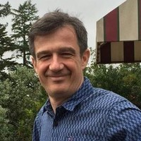 Martin Kuball合作论文数University of Bristol17
 Fedor Jelezko合作论文数Institute for Quantum Optics, Ulm University;Department of Physics, Ulm University16S. J. Rashid合作论文数15
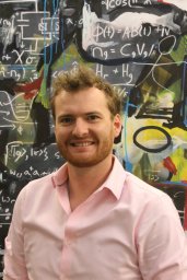 Machiel S. Blok合作论文数Kavli Institute of Nanoscience Delft, Delft University of Technology;Kavli Institute of Nanoscience Delft, Delft University of Technology15
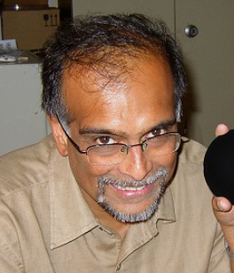 Gehan Amaratunga合作论文数Grainger College of Engineering, Zhejiang University - University of Illinois Urbana-Champaign Institute;Department of Engineering, University of Cambridge15
 Florin Udrea合作论文数Department of Engineering, University of Cambridge15
 Daniel Francis合作论文数15
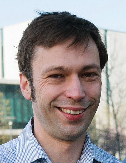 Hannes Bernien合作论文数Pritzker School of Molecular Engineering, The University of Chicago14
 Saman Majdi合作论文数Division For Electricity Research Box, Uppsala University14
 James Pomeroy合作论文数School of Physics, University of Bristol13
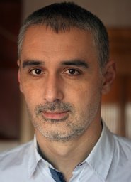 Mihai Brezeanu合作论文数Department of Inorganic Chemistry, Bucharest University13A.J. Whitehead合作论文数13T. Butler合作论文数13
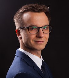 Norbert Kalb合作论文数QuTech, Delft Univ Technol12
 Nalin Rupesinghe合作论文数Department of Engineering, University of Cambridge12
 Andrew Edmonds合作论文数Element Six12A. Garraway合作论文数11
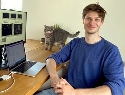 C. E. Bradley合作论文数Delft Univ Technol, QuTech, POB 5046, NL-2600 GA Delft, Netherlands11J.M. Dodson合作论文数11
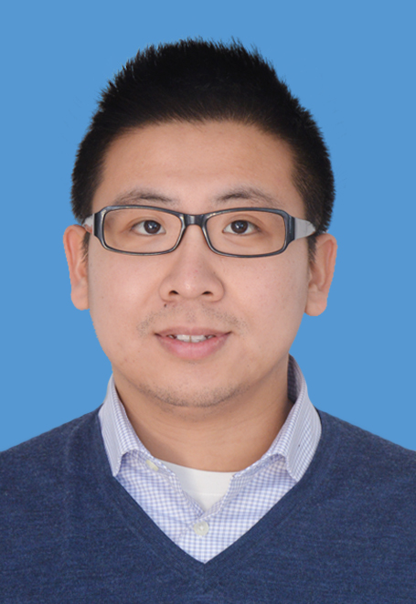 Huarui Sun (孙华锐)合作论文数School of Science, Harbin Institute of Technology, Shenzhen10P. Taylor合作论文数10Thomas R Anthony合作论文数10R. U. A. Khan合作论文数9M. H. Abobeih合作论文数Delft Univ Technol, QuTech, NL-2600 GA Delft, Netherlands9
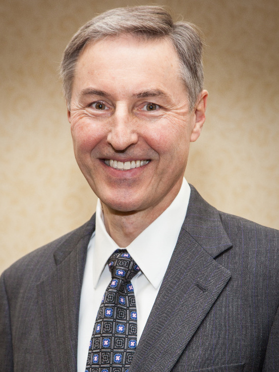 William F. Banholzer合作论文数University of Wisconsin-Madison9
 Dirk Englund合作论文数Department of Electrical Engineering and Computer Science, Schwarzman College of Computing, Massachusetts Institute of Technology;LightMatter Computing Inc;Dust Identity Inc9
 Alastair Stacey合作论文数School of Physics, University Of Melbourne9Vladimir A. Nadolinny合作论文数9
 Lee Coulbeck合作论文数9D. Francis合作论文数8
 Joe Randall合作论文数8H. P. Bartling合作论文数Delft Univ Technol, QuTech, Delft, Netherlands8M. J. Degen合作论文数Delft Univ Technol, QuTech, POB 5046, NL-2600 GA Delft, Netherlands8Roland B Simon合作论文数8
 Edward H. Chen合作论文数8




