A $6+$ GHz multi-port 10T Ground Rule Clean (GRC) compact Cache is implemented in the recently announced IBM Telum II processor [1]. It features a Multi port design (2 Read and 1 Write) with fine grain banked architecture minimizing read and write collisions. The design is functional across various corner conditions without read and write assist circuits.
The IBM z15 system improves upon the prior-generation z14 design within the same chip footprint and technology node, while featuring the addition of two cores, 33%/100%/43% additional L2/L3/L4 cache, as well as additional core features and on-chip accelerators. The largest 5-drawer system configuration includes 20 central processor (CP) chips, five system controller (SC) chips, and 40 TB of memory. With ~200 cores across all CP chips operating with 99.99999% uptime at 5.2 GHz, z15 achieves a 25% increase in system capacity and a 14% single thread performance improvement over the z14 system. In this article, we describe the key design factors and system/characterization refinement that enabled these results, including the novel 2-Mb embedded dynamic random access memory (eDRAM) cell, a new voltage droop monitor, a more comprehensive power reduction infrastructure to reduce power-limited yield, results on reliability-limited versus power-limited yield, and a characterization effort for exploring even higher frequencies, with our first reported 6-GHz values achieved in the lab at customer temperatures and voltages.
The latest IBM Z microprocessor in the z15 system has been redesigned to have improved performance, system capacity and security over the previous z14 system [1]. These achievements are made while maintaining the central processor (CP) and system controller (SC) chip die sizes at 696mm 2 in the GlobalFoundries 14nm high performance (14HP) SOI FinFET technology and 17 layers of copper interconnect [2], both design points of the z14 system. The system contains up to 20 CP and 5 SC chips. Each CP, shown in die photo A (Fig. 2.7.7), operates at 5.2GHz and is comprised of 12 cores, 3 PCle Gen4 interfaces, 256MB of L3 embedded DRAM (eDRAM) cache, two X-BUS interfaces connecting to one other CP chip and one SC chip, and a redundant array of independent memory (RAIM) interface. Each core on the CP chip has 8MB of L2 eDRAM cache as well as 256KB of L1 SRAM cache, both caches split evenly between data and instruction. Each SC, shown in die photo B, operates at half the frequency of the CP, or 2.6GHz, has 960MB of L4 eDRAM cache, X-BUS interfaces connecting to half of the CP chips in the drawer and four A-BUS interfaces connecting to the SC chips on the other drawers in the system. The CP contains 9.2B transistors and the SC contains 12.2B transistors. The total 10 bandwidth of the CP and SC are 2.3Tb/s and 5.6Tb/s, respectively.
A 1.1 Mb embedded DRAM macro (eDRAM), for next-generation IBM SOI processors, employs 14 nm FinFET logic technology with 0.0174 μm 2 deep-trench capacitor cell. A Gated-feedback sense amplifier enables a high voltage gain of a power-gated inverter at mid-level input voltage, while supporting 66 cells per local bit-line. A dynamic-and-gate-thin-oxide word-line driver that tracks standard logic process variation improves the eDRAM array performance with reduced area. The 1.1 Mb macro composed of 8 ×2 72 Kb subarrays is organized with a center interface block architecture, allowing 1 ns access latency and 1 ns bank interleaving operation using two banks, each having 2 ns random access cycle. 5 GHz operation has been demonstrated in a system prototype, which includes 6 instances of 1.1 Mb eDRAM macros, integrated with an array-built-in-self-test engine, phase-locked loop (PLL), and word-line high and word-line low voltage generators. The advantage of the 14 nm FinFET array over the 22 nm array was confirmed using direct tester control of the 1.1 Mb eDRAM macros integrated in 16 Mb inline monitor.
James Warnock, Brian Curran, John Badar, Gregory Fredeman, Donald Plass, Yuen Chan, Sean Carey, Gerard Salem, Friedrich Schroeder, Frank Malgioglio, Guenter Mayer, Christopher Berry, Michael Wood, Yiu-Hing Chan, Mark Mayo, John Isakson, Charudhattan Nagarajan, Tobias Werner, Leon Sigal, Ricardo Nigaglioni, Mark Cichanowski, Jeffrey Zitz, Matthew Ziegler, Tim Bronson, Gerald Strevig, Daniel Dreps, Ruchir Puri, Douglas Malone, Dieter Wendel, Pak-Kin Mak, Michael Blake
IBM introduced trench capacitor eDRAM into its high performance microprocessors beginning with 45nm and Power 7 [1] to provide a higher density cache without chip crossings. Whereas the 45 and 32nm designs employ a micro sense amplifier [2] and three-level bitline hierarchy, the design implemented for 22nm utilizes a higher gain sense amplifier and two-level bitline architecture that together provide significant reductions in area, latency, and power. This 22nm design style has been migrated into a 14nm FinFET [3] learning vehicle, complete with an ABIST engine, wordline charge pumps (VPP and VWL), and padcage interface circuitry.
A 1.35 ns random access and 1.7 ns-random-cycle SOI embedded-DRAM macro has been developed for the POWER7™ high-performance microprocessor. The macro employs a 6 transistor micro sense-amplifier architecture with extended precharge scheme to enhance the sensing margin for product quality. The detailed study shows a 67% bit-line power reduction with only 1.7% area overhead, while improving a read zero margin by more than 500ps. The array voltage window is improved by the programmable BL voltage generator, allowing the embedded DRAM to operate reliably without constraining of the microprocessor voltage supply windows. The 2.5nm gate oxide transistor cell with deep-trench capacitor is accessed by the 1.7 V wordline high voltage (VPP) with V WL low voltage (VWL), and both are generated internally within the microprocessor. This results in a 32 MB on-chip L3 on-chip-cache for 8 cores in a 567 mm POWER7™ die.
Logic-based embedded DRAM has matured into a wide range of ASIC applications, SRAM replacements [1] and off-chip caches for microprocessors [2]. While embedded DRAM has been leveraged in supercomputers such as IBM's BlueGene/L [3], it's use has been limited to moderate performance bulk logic technologies. Although prototypes have been demonstrated [4], DRAM has yet to be embedded on a high performance microprocessor. This paper discloses an SOI DRAM macro implemented on-chip with the IBM POWER7™ high performance microprocessor [5], and introduces enhancements to the micro sense amp (µSA) architecture [6]. This high performance DRAM macro is used to construct a large 32MB L3 cache on-chip, eliminating delay, area and power from the off-chip interface, simultaneously improving system performance, reducing cost, power and soft error vulnerability. Figure 19.1.1a shows an SEM of the 45nm SOI DRAM Device and Deep Trench (DT) capacitor [7]. DT offers 25x more capacitance than planar structures and was also utilized to reduce on-chip voltage island supply noise.
We describe a single voltage supply, 1 MB cache subsystem prototype that integrates 2 GHz embedded DRAM (eDRAM) macros with on-chip word-line voltage supply generation , a 4 Kb one-time-programmable read-only memory (OTPROM) for redundancy and repair control, on-chip OTPROM programming voltage generation, clock generation and distribution, array built-in self-test circuitry (ABIST), user logic and pervasive logic. The eDRAM employs a programmable pipeline, achieving 1.8 ns latency, and features concurrent refresh capability.
We present a 1 MB cache subsystem that integrates 2 GHz embedded DRAM macros, charge pump circuits, a 4 Kb one-time-programmable ROM, clock multipliers, and built-in self test circuitry, having a 36.5 GB/s peak system data-rate. The eDRAM employs a programmable pipeline, achieving a 1.8 ns latency.
 Toshiaki Kirihata合作论文数IBM Systems and Technology Group, Semiconductor Research and Development Center, 2070 Route 52, Hopewell Junction, NY 12533, USA14
 Abraham Mathews合作论文数8
 Donald W. Plass合作论文数7
 Mark Cichanowski合作论文数IBM Syst & Technol, Austin, TX USA6
 John Isakson合作论文数6
 Christopher J. Berry合作论文数6
 Alan Leslie合作论文数New York6
 Paul C. Parries合作论文数6
 John Golz合作论文数6john e barth合作论文数5William R. Reohr合作论文数5
 Subramanian S. Iyer合作论文数Department of Electrical and Computer Engineering, Samueli School of Engineering, University of California5John M Safran合作论文数5louis l hsu合作论文数4
 Sean Carey合作论文数4
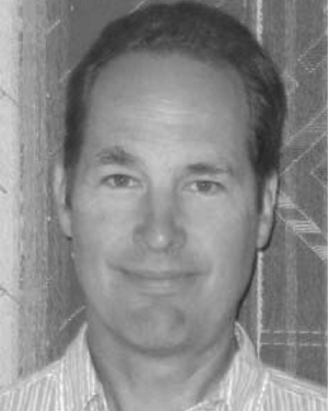 Erik Nelson合作论文数4
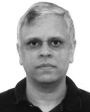 Dureseti Chidambarrao合作论文数ibm4
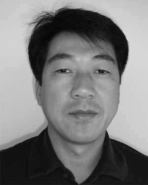 Hoki Kim合作论文数Princeton and Telcordia Technologies, Inc.4david r hanson合作论文数3
 Brian Bell合作论文数3
 Jesse Surprise合作论文数3
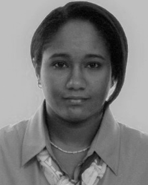 Dina Hamid合作论文数3
 Chris Cavitt合作论文数IBM Syst, Hardware Dev Team, Poughkeepsie, NY 12601 USA3
 Brandon Bruen合作论文数IBM Systems and Technology,Pouahkeepsie,NY3
 Brian Deskin合作论文数3
 Ofer Geva合作论文数3
 Preetham Lobo合作论文数3
 Ashutosh Mishra合作论文数Sch Phys, Devi Ahilya Univ3Ricardo Nigaglioni合作论文数3John Badar合作论文数3
 Michael Sperling合作论文数3David H. Wolpert合作论文数Department of Electrical and Computer Engineering;University of Rochester;School of Engineering and Applied Sciences3Darren Anand合作论文数3
 Ramon Bertran Monfort合作论文数IBM3
 Ruchir Puri合作论文数IBM Research3Leon J. Sigal合作论文数3
 Adam Jatkowski合作论文数3
 Tobias Webel合作论文数IBM;IBM Deutschland Research & Development GmbH3
 Alper Buyuktosunoglu合作论文数Efficient and Resilient Systems Department, IBM Thomas J. Watson Research Center3
 Hillery Hunter合作论文数Systems Acceleration and Memory at IBM3Frank Malgioglio合作论文数3
 Anthony Saporito合作论文数3Jeffrey A. Zitz合作论文数3Brian W. Curran合作论文数3Guenter Mayer合作论文数3
 Dieter Wendel合作论文数3Friedrich Schroeder合作论文数2Douglas Malone合作论文数2Charudhattan Nagarajan合作论文数2




