Recent advances in semiconductor processing technology have enabled development of a solid-state neutron sensor with exceptional efficiency for its unique reduced size. The boron-10 (n, alpha) capture reaction is used to detect incident thermal neutrons. This reaction offers significant advantages for a small detector because the reaction products have high energies which can generate a large number of charge carriers in semiconductor materials by impact ionization. The enabling and differentiating technology of the sensor design is a stack consisting of multiple bilayers alternating between converter material (boron) and collector semiconductor material (silicon). As the number of these bilayers increases, the probability of a neutron interacting with boron-10 in at least one of the bilayers-so it is captured in the detector before it has a chance to pass through-approaches unity. The sensor can be made very thin while also remaining highly efficient, offering a unique possibility for low-profile in situ dosimetry. Calculations have shown that a multilayer sensor with an efficiency greater than 70% is feasible in a sensor stack 2 mm thick.
Manufacturing of integrated circuits (ICs) using a split foundry process expands design space in IC fabrication by employing unique capabilities of multiple foundries and provides added security for IC designers [1]. Defect localization and root cause analysis is critical to failure identification and implementation of corrective actions. In addition to split-foundry fabrication, the device addressed in this publication is comprised of 8 metal layers, aluminum test pads, and tungsten thru-silicon vias (TSVs) making the circuit area > 68% metal. This manuscript addresses the failure analysis efforts involved in root cause analysis, failure analysis findings, and the corrective actions implemented to eliminate these failure mechanisms from occurring in future product.
We demonstrate a front-side process integration method to insert high-density 1.2um diameter Tungsten (W) Through Silicon Vias (TSVs) into advanced-node logic wafers after metal-4. This late-TSV-middle approach offers the ability to build 3D technology into commercially available 90nm-node CMOS, while avoiding many of the challenges associated with TSV-last integrations. We also demonstrate a TSV-reveal process compatible with small-diameter W TSVs.
Quantum dot (QD) layouts are becoming more complex as the technology is being applied to more sophisticated multi-QD structures. This increase in complexity requires improved capacitance modeling both for the design and accurate interpretation of QD properties from measurement. A combination of process simulation, electrostatic simulation, and computer-assisted design (CAD) layout packages are used to develop a 3-D classical capacitance model. The agreement of the classical model's capacitances is tested against two different, experimentally measured, topographically complex silicon QD geometries. Agreement with experiment, within 10%-20%, is demonstrated for the two structures when the details of the structure are transferred from the CAD to the model capturing the full 3-D topography. Small uncertainties in device dimensions due to uncontrolled variation in processing, like layer thickness and gate size, are calculated to be sufficient to explain the disagreement. The sensitivity of the capacitances to small variations in the structure also highlights the limits of accuracy of capacitance models for QD analysis. We furthermore observe that a critical density, the metal-insulator transition, can be used as a good approximation of the metallic edge of the QD when electron density in the dot is calculated directly with a semiclassical simulation.
When designing and studying circuits operating at cryogenic temperatures understanding local heating within the circuits is critical due to the temperature dependence of transistor and noise behavior. Local heating effects of a CMOS ring oscillator and current comparator were investigated at T=4.2K. In two cases, the temperature near the circuit was measured with an integrated thermometer. A lumped element equivalent electrical circuit SPICE model that accounts for the strongly temperature dependent thermal conductivities and special 4.2K heat sinking considerations was developed. The temperature dependence on power is solved numerically with a SPICE package, and the results are typically within 3σ of the measured values for local heating ranging from <1K to over 100K.
In this paper we present the impact of classical electronics constraints on a solid-state quantum dot logical qubit architecture. Constraints due to routing density, bandwidth allocation, signal timing, and thermally aware placement of classical supporting electronics significantly affect the quantum error correction circuit's error rate. We analyze one level of a quantum error correction circuit using nine data qubits in a Bacon-Shor code configured as a quantum memory. A hypothetical silicon double quantum dot quantum bit (qubit) is used as the fundamental element. A pessimistic estimate of the error probability of the quantum circuit is calculated using the total number of gates and idle time using a provably optimal schedule for the circuit operations obtained with an integer program methodology. The micro-architecture analysis provides insight about the different ways the electronics impact the circuit performance (e.g., extra idle time in the schedule), which can significantly limit the ultimate performance of any quantum circuit and therefore is a critical foundation for any future larger scale architecture analysis.
Coherent Tunneling Adiabatic Passage (CTAP) has been proposed as a long-range physical qubit transport mechanism in solid-state quantum computing architectures. Although the mechanism can be implemented in either a chain of quantum dots or donors, a 1D chain of donors in Si is of particular interest due to the natural confining potential of donors that can in principle help reduce the gate densities in solid-state quantum computing architectures. Using detailed atomistic modeling, we investigate CTAP in a more realistic triple donor system in the presence of inevitable fabrication imperfections. In particular, we investigate how an adiabatic pathway for CTAP is affected by donor misplacements, and propose schemes to correct for such errors. We also investigate the sensitivity of the adiabatic path to gate voltage fluctuations. The tight-binding based atomistic treatment of straggle used here may benefit understanding of other donor nanostructures, such as donor-based charge and spin qubits. Finally, we derive an effective 3 \times 3 model of CTAP that accurately resembles the voltage tuned lowest energy states of the multi-million atom tight-binding simulations, and provides a translation between intensive atomistic Hamiltonians and simplified effective Hamiltonians while retaining the relevant atomic-scale information. This method can help characterize multi-donor experimental structures quickly and accurately even in the presence of imperfections, overcoming some of the numeric intractabilities of finding optimal eigenstates for non-ideal donor placements.
Negligible population at CTAP pulsing scheme • Goal: Develop a small scale (3x3) model that encapsulates the atomistic TB information. • Advantages: Optimal voltages can be obtained analytically from this parameterized model. Possible to simulate many configurations very fast to guide experiments. • Approach: Use single donor TB wfs as basis for 3x3 model. Treat gate biases as perturbations & project full Hamiltonian on the single donor basis. Parameterize the matrix elements to characterize gate control. Find (VS1, VB1, VB2, VS2) that recovers original Hamiltonian
We present and analyze an architecture for a logical qubit memory that is tolerant of faults in the processing of silicon double quantum dot (DQD) qubits. A highlight of our analysis is an in-depth consideration of the constraints faced when integrating DQDs with classical control electronics.
Novel single electron transistor (SET) read-out circuit designs are described. The circuits use a silicon SET interfaced to a CMOS voltage mode or current mode comparator to obtain a digital read-out of the state of the qubit. The design assumes standard submicron (0.35 um) CMOS SOI technology using room temperature SPICE models. Implications and uncertainties related to the temperature scaling of these models to 100mK operation are discussed. Using this technology, the simulations predict a read-out operation speed of approximately Ins and a power dissipation per cell as low as 2nW for single-shot read-out, which is a significant advantage over currently used radio frequency SET (RF-SET) approaches.
Thesis (M.S.), School of Electrical Engineering and Computer Science, Washington State University
Pipelining digital systems has been shown to provide significant performance gains over non-pipelined systems and remains a standard in microprocessor design. The desire for increased performance has seen a push for deeper pipelines, as well as the introduction of pipelining schemes such as wave-pipelining and hybrid wave-pipelining. In this paper we present a hybrid wave-pipelined parallel adder that operates at 1.79 GHz, 42% performance improvement compared to that of a superpipelined adder. The simulations have been performed using a modest 0.25 mum technology. The three stage hybrid wave-pipelined parallel adder sustains a total of 8 unrelated data waves within the pipe. Another performance benefit achieved by using the hybrid wave-pipelining scheme is the lessening of delays associated with clock skew and clock distribution
Adders are some of the most critical data path circuits requiring considerable design effort in order to “squeeze” out as much performance gain as possible. Many adder designs manage high performance by reducing the delay of the critical path, an effort that results in high area overhead in most cases. In this paper we present a carry lookahead adder (CLA) with a prediction scheme that results in improved performance and low area overhead. Carry prediction enables for the reduction of the carry circuitry within a block while reducing the delay involved in the generation of the carry-out to the subsequent blocks. We have performed simulations of a 16-bit adder and recorded performance improvements of 67% in propagating the carry and generating the sum when compared with the traditional (fixed group4) CLA designed in the same technology.
 Malcolm Carroll合作论文数IBM8
 Thomas M. Gurrieri合作论文数5Daniel Dorsey合作论文数2Douglas Nichols合作论文数2David Adams合作论文数2Adam Jones合作论文数2Lovelace Soirez合作论文数2
 Liam Claus合作论文数2harold l stalford合作论文数2Richard Harrison合作论文数Department of Mechanical Engineering, University of Texas at Austin2
 Andrew Greentree合作论文数ARC Centre of Excellence for Nanoscale BioPhotonics, RMIT University;School of Science, RMIT University2
 Lloyd Hollenberg合作论文数Division of Science, University of Melbourne;Australian Institute of Physics, University of Melbourne2
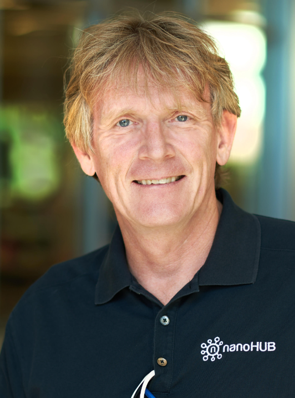 Gerhard Klimeck合作论文数Center for Predictive Materials and Devices, Elmore Family School of Electrical and Computer Engineering, Purdue University2
 Anand Ganti合作论文数2
 Rajib Rahman合作论文数School of Physics, Faculty of Science, The University of New South Wales2Robert D. Carr合作论文数2
 Cynthia Ann Phillips合作论文数Center for Computing Research, Sandia National Laboratories2Jason R. Hamlet合作论文数2
 Andrew J. Landahl合作论文数Center for Quantum Information and Control, The University of New Mexico;Department of Physics & Astronomy, The University of New Mexico;Sandia National Laboratories2
 Jabulani Nyathi合作论文数Eastern Washington University2Ralph W. Young合作论文数2Kenton D. Childs合作论文数1mark w jenkins合作论文数1edward cole jr i合作论文数1Douglas C. Trotter合作论文数Sandia National Laboratories1Kevin Eng合作论文数1
 Matthew B. Jordan合作论文数1Nielsen Erik合作论文数1
 Carlos Borras合作论文数1T. Gurrieri合作论文数1
 Jeremy A. Walraven合作论文数Sandia National Laboratories1
 Jose G. Delgado-Frias合作论文数Washington State University;School of Electrical Engineering and Computer Science1E. P. Nordberg合作论文数1Benjamin R. Hamlet合作论文数1
 Michael Lilly合作论文数Caltech1
 Richard S. Muller合作论文数Electrical Engineering and Computer Sciences Department, College of Engineering, University of California, Berkeley;Berkeley Sensor & Actuator Center, College of Engineering, University of California1




