A residue-free interface and strong light–matter coupling are crucial for achieving high-performance 2D photodetectors. Here, a MoSSe/GeP heterostructure is fabricated using an Elvacite pickup transfer strategy, enabling a clean van der Waals junction and contamination-free electrical contacts. Structural and spectroscopic characterizations, including AFM, Raman spectroscopy, and Raman mapping, collectively confirm high crystalline quality, uniform layer thickness, and a chemically sharp interface. Electrical transport measurements further show that GeP exhibits p-type behavior, whereas Janus MoSSe displays n-type conduction, thereby confirming their suitability as complementary semiconductors for p-n junction formation. The pristine p-n junction device exhibits strong rectification (2.2 × 10³ at Vg = − 40 V). After sensitization with lead-free perovskite quantum dots (λem ≈ 510 nm), the QD-MoSSe/GeP heterostructure exhibits a pronounced built-in field-driven photocurrent of approximately 0.25 µA at zero bias, confirming efficient interfacial separation. QD integration enhances responsivity, detectivity, and EQE from 1.64 × 10⁴ AW-1, 3.55 × 10¹³ Jones, and 2.36 × 10⁴
Two-dimensional (2D) layered materials have gained significant attention as candidates for field-effect transistors (FETs) in next-generation electronics and ultrafast memory applications for artificial intelligence (AI) systems. In this study, we present a reliable and efficient approach to fabricate a photonic synaptic transistor for neuromorphic and reservoir computing, achieved by utilizing oxygen plasma treatment on the bottom side of hafnium disulfide (HfS2). The fabricated device exhibits n-type semiconducting characteristics and a pronounced clockwise hysteresis in its transfer curves, which is attributed to intentionally engineered defect-induced traps within the HfOx layer. Notably, the device exhibits a substantial memory window of approximately 114 V during a gate voltage sweep of ± 100 V, and the memory window can be dynamically tuned from 4 V to 114 V by adjusting the gate voltage sweep range between ± 10 V and ± 100 V. Furthermore, the device exhibits low energy consumption of 2.25 nJ per optical spike, demonstrating its suitability for low-power neuromorphic systems. Additionally, the device demonstrates core synaptic behaviors including paired-pulse facilitation (PPF), excitatory postsynaptic current (EPSC), optical spike number dependent plasticity (SNDP), and spike time dependent plasticity (STDP) under ultraviolet illumination (365 nm). The device further achieves 32 distinct output states, highlighting its suitability for 5-bit reservoir computing systems. These results provide an innovative approach for advancing AI-based hardware and efficient computing platforms.
Janus materials are an emerging class of two-dimensional materials with a diversity of two exclusive sides, which embark on various new multifunctional properties for electronics, optoelectronics, and memory application devices. Evolving technologies like neuromorphic computing based on floating-gate transistors, architecting an advanced artificial intelligence technology (AIT) to emulate efficient brain-like synaptic functions. In this study, we present an emerging memory design using Au/hBN/WSSe and Gr/hBN/WSSe heterostructures on the same WSSe channel, where gold and graphene serve as floating-gate materials and hexagonal boron nitride (h-BN) as an effective tunneling layer. By comparing the performance metrics based on device configurations under controlled conditions, we achieved a current ON/OFF ratio (similar to 10(5)) and (similar to 10(3)) for Au and few layer graphene as floating gates, respectively. The memory devices with Gr floating gate demonstrated the significant and consistent memory window of Delta V = 65 V compared to Au (Delta V = 51 V). Further, Gr/hBN/WSSe showed promising endurance (10(5) cycles) and retention (10(6) s), having gate-dependent multi-states for erase and program. Moreover, we used an artificial neural network (ANN) for digit-MNIST and Fashion-MNIST simulations, which achieved 87 % and 78 % accuracy, respectively. Simulations of WSSe-based synaptic transistors further demonstrate their capability to support ANN learning, underscoring the potential of this platform to drive next-generation AIT for memory and computing systems.
Nano-devices based on two-dimensional (2D) semiconductor materials encourage the development of high-performance homogeneous junctions owing to their remarkable electronic and optoelectronic properties. Herein, we fabricated an atomically thin WSe2 (similar to 4.8 nm) lateral homojunction PN diode through the deposition of indium gallium zinc oxide (IGZO) via sputtering. Pristine WSe2 exhibited dominant p-type semiconductor behavior, while IGZO-deposited WSe2 demonstrated n-type behavior, revealing that IGZO altered the carrier polarity of WSe2 from p- to n-type. Furthermore, we investigated gate-dependent I-V curves of the lateral homojunction PN (p-WSe2/n-IGZOWSe2) diode in the dark based on a single WSe2 flake, which showed a promising current rectification ratio (similar to 1.6 x 10⁴) and ideality factor (similar to 1.23) at VBG = -30 V, respectively. Subsequently, to explore the photodiode characteristics, we irradiated the lateral homojunction PN diode of WSe2 under ultra-violet (UV) to near-infrared (NIR) light (365, 530, and 850 nm). The I-V curves of the diode significantly changed under light irradiation, and the open circuit voltage (Voc = 202, 166, and 134 mV) and short circuit current (Isc = 320, 171, and 122 nA) values increased under illumination of a laser of small wavelength (365, 530, and 850 nm). Furthermore, we investigated the time-dependent photoresponse behavior of the diode under different laser lights. This demonstrated promising photoresponsivity (RPh = 40.1 A W-1) and external quantum efficiency (EQE = 13 634%) at lambda = 365 nm and VBG = 15 V. Hence, our lateral homojunction PN diode WSe2-IGZO/WSe2 shows great potential for next-generation electronic devices at the nanoscale level.
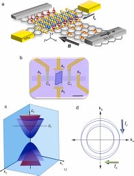
Spintronics seeks to enhance information processing by harnessing the spin of electrons, offering solutions to the limitations of conventional electronics. A key device in spintronics research is the spin-injected field-effect transistor (spin FET), which incorporates a lateral semiconducting channel and ferromagnetic electrodes. This study presents a high-mobility BLG/WSe2/hBN spin FET capable of operating from cryogenic to room temperature, demonstrating efficient spin injection, detection, and precession. We investigate spin transport across different transport regimes, revealing coherent spin precession in the ballistic regime and a transition to reduced coherence in the semiballistic and diffusive regimes. By modulating the gate voltage, we achieve precise control over Rashba spin-orbit coupling, which enables tunable spin dynamics in the device. These findings advance the understanding of spin transport in 2D heterostructures and pave the way for developing electrically controlled spintronic devices for future applications in logic, memory, and quantum technologies.
Correction for 'Broadening spectral responses and achieving environmental stability in SnS2/Ag-NPs/HfO2 flexible phototransistors' by Muhammad Farooq Khan et al., Nanoscale, 2024, 16, 3622-3630, https://doi.org/10.1039/D3NR04626E.
Non-volatile memory devices, which offer large capacity and mechanical dependability as a mainstream technology, have played a key role in fostering innovation in modern electronics. Despite the advantages of non-volatile memory devices, their low ON/OFF ratio and slow operational speed have limited their performance compared to their volatile counterparts. In this study, we present a non-volatile floating-gate memory device based on van der Waals heterostructures, which exhibits ultrahigh-speed memory operations in the range of a hundred nanoseconds with an extinction ratio of up to 106. The device consists of atomically sharp interfaces between different functional elements, including atomically thin sheet of multilayer Graphene (MGr) as a floating gate, hexagonal boron nitride (h-BN) as a tunnel barrier, and two-dimensional (2D) semiconductor tin di-selenide (SnSe2) as a channel material. The memory device exhibits excellent endurance performance with stable and dependable behavior across numerous program/erase cycles, comparable to commercial volatile dynamic random access memory technology. In addition, we demonstrate the ability of the device to store multiple bits per memory cell, which offers promising potential for ultrahigh-density information storage. Our findings provide important implications for memory storage, data processing, and electronic device development, and offer new opportunities in the field of emerging 2D materials with optimal device engineering.
Field effect transistors based on 2D layered material have gained significant potential in emerging technologies, such as neuromorphic computing and ultrafast memory response for artificial intelligence applications. This study proposes a facile approach to fabricate an optoelectronic artificial synapse for neuromorphic computing and light-decoding information system by utilizing the 2D heterostructure of CrSBr/PtS2 to overcome circuit complexity. The CrSBr layer serves as a trapping layer, while PtS2, mounted on top of CrSBr, acts as a channel layer. PtS2 exhibits n-type semiconductor behavior with a hysteresis that varies with the thickness of the underlying CrSBr layer. The heterostructure device, featuring a 96.3 nm thick CrSBr layer, exhibited a large memory window of 11.9 V when the gate voltage is swept from -10 V to +10 V. Various synaptic behaviors are effectively demonstrated, including paired-pulse facilitation, excitatory postsynaptic current, optical spike number and intensity-dependent plasticity using laser light at a wavelength of 365 nm. The device achieves 26 distinct output signals depending on the intensity of the incident laser light, ranging from 10 to 385 mW cm(-2), enabling its applications for light-decoded information security systems. Thus, the investigation presents a unique approach to artificial intelligence and cybersecurity systems.
Perovskite solar cells (PSCs) are transforming the renewable energy sector with their remarkable efficiencies and economical large-scale manufacturing. Perovskite materials have earned significant attention for their unique properties, including high light absorption, efficient charge transport, and ease of fabrication. These unique features of perovskite materials are essential for developing high-efficiency PSCs, which are considered leading candidates for sustainable energy solutions. This review comprehensively analyzes high-efficiency PSCs, focusing on their critical aspects such as perovskite material properties, device configurations, fabrication techniques, and the latest advancements. Our review addresses vital factors such as stability concerns, environmental impact, production scalability, device reproducibility, and challenges related to perovskite degradation that are pertinent to the advancement of PSC technology. Additionally, we discuss emerging trends in tandem and multijunction devices, flexible and wearable applications, and the integration of PSCs into building-integrated photovoltaic systems. Furthermore, we examine limitations, challenges, and future prospects for PSCs, including developing improved stability protocols, enhancing efficiency, and integrating energy storage solutions to drive advancements in PSC manufacturing. Lastly, we provide insights into the commercialization pathway for inverted PSCs, underscoring the importance of stability, cost reduction, and efficiency enhancement in achieving widespread adoption of this promising technology.
The decoration of Ag-NPs and passivation with HfO 2 provide a simple route to realize broadband and stable photoactivity in SnS 2 photodetectors.
The rapid advancement of artificial intelligent and information technology has led to a critical need for extremely low power consumption and excellent efficiency. The capacity of neuromorphic computing to handle large amounts of data with low power consumption has garnered a lot of interest during the last few decades. For neuromorphic applications, 2D layered semiconductor materials have shown a pivotal role due to their distinctive properties. This comprehensive review provides an extensive study of the recent advancements in 2D materials‐based neuromorphic devices especially in multiterminal synaptic devices, two‐terminal synaptic devices, neuronal devices, and the integration of synaptic and neuronal devices. Herein, a wide range of potential applications of memory, computation, adaptation, and artificial intelligence is incorporated. Finally, the limitations and challenges of neuromorphic devices based on novel 2D materials are discussed. Thus, this review aims to illuminate the design and fabrication of neuromorphic devices based on van der Waals (vdW) heterostructure materials, leveraging promising engineering techniques to excel the applications and potential of neuromorphic computing for hardware implementations.
Nanoscale photonics of atomically thin layered two-dimensional (2D) materials and their integrations have been comprehensively investigated owing to their unique electronic, mechanical, and optical properties. The prospective selection of emerging 2D materials and their van der Waals heterostructures (vdWHs) enable it to be an auspicious approach for a variety of self-driving optoelectronics. However, self-powered photodetectors (SPPDs) manifested by 2D materials MXene and perovskite have drawn considerable attention due to their massive potential for energy-efficient and cost-effective devices. In this review, to begin with, we summarized the recent innovations of SPPD architectures based on transition metal dichalcogenides (TMDCs), MXene and perovskite materials. The unique configuration of SPPDs is classified into various categories of a single material, homojunction, heterojunction, Schottky junction, and flexibility. In addition, the working principles of SPPD and their performance metrics such as detectivity, responsivity, noise equivalent power and their outstanding applications for the modern era have been demonstrated. To conclude we focused on the numerous challenges and future perspectives of this rapidly evolving research area. Overall, this review provides a comprehensive analysis of recent innovations in self-powered SPPDs made from novel materials, contributing to the diversity of the nano-photonic industry.
Emerging technologies such as neuromorphic computing and nonvolatile memories based on floating gate field-effect transistors (FETs) hold promise for addressing a wide range of artificial intelligence tasks. For example, neuromorphic computing seeks to emulate the human brain's functionality and employs a device that mimics the role of a synapse in the brain. However, achieving a high current ON/OFF ratio for the program and erase states of nonvolatile memory and neuromorphic computing device with a metal gate is necessary. This study demonstrates a multi-functional device based on heterostructures of transition metal dichalcogenides (TMDCs) with a metal floating gate. Five different channel materials (SnS2, WSe2, MoS2, WS2, and MoTe2) were employed, and hexagonal boron nitride (h-BN) was used as a tunneling layer. The study found that n-type SnS2 exhibits high endurance (15,000 cycles), good retention (2.4 × 10⁵ s), and the highest current ON/OFF ratio (∼2.58 × 10⁸) among the materials for the program and erase states. Moreover, the SnS2 device exhibits synaptic behavior and offers highly stable operation at room temperature. Furthermore, the device shows high linearity in both potentiation and depression, with good retention time and repeatable results with low cycle-to-cycle variations. Additionally, the study used an artificial neural network (ANN) for MNIST simulation of image recognition and achieved the highest accuracy of ∼92 % based on the SnS2 synaptic device experimental results. These findings pave the way for developing nonvolatile memory devices and their applications in brain-inspired neuromorphic computing and artificial intelligence systems.
In this research, it is aimed to obtain and to compare the electrical conductivity and the transmittance of two graphene (Gr)‐based heterostructures: Gr/WS 2 and Gr/MoS 2 on quartz. Raman spectroscopy is used to analyze the quality of the samples before and after the measurements. Terahertz time domain spectroscopy in transmission mode is used as a nondestructive technique to obtain the surface conductivity and the transmittance in the frequency range [0.2, 1.6] THz. The transmittance values obtained for both samples are similar, whereas the surface conductivity of Gr/WS 2 is higher than the one of Gr/MoS 2 and both are higher than the conductivity values obtained for individual homogeneous layers. Fourier transform infrared spectroscopy and UV–Vis spectroscopies are used to obtain the optical transmittance and to evaluate the behavior of each layer in the frequency ranges [90, 180] and [300, 1200] THz, respectively. In the infrared range, the transmittance of the heterostructures is similar to that of the individual materials, although in the visible range the transmittance is totally dominated by the WS 2 and MoS 2 layers. These characteristics make these heterostructures good candidates to be used for optoelectronics sensors.
To avoid the complexity of the circuit for in‐memory computing, simultaneous execution of multiple logic gates (OR, AND, NOR, and NAND) and memory behavior are demonstrated in a single device of oxygen plasma‐treated gallium selenide (GaSe) memtransistor. Resistive switching behavior with R ON /R OFF ratio in the range of 10 4 to 10 6 is obtained depending on the channel length (150 to 1600 nm). Oxygen plasma treatment on GaSe film created shallow and deep‐level defect states, which exhibit carriers trapping/de‐trapping, that lead to negative and positive photoconductance at positive and negative gate voltages, respectively. This distinguishing feature of gate‐dependent transition of negative to positive photoconductance encourages the execution of four logic gates in the single memory device, which is elusive in conventional memtransistor. Additionally, it is feasible to reversibly switch between two logic gates by just adjusting the gate voltages, e.g., NAND/NOR and AND/NAND. All logic gates presented high stability. Additionally, memtransistor array (1×8) is fabricated and programmed into binary bits representing ASCII (American Standard Code for Information Interchange) code for the uppercase letter “N”. This facile device configuration can provide the functionality of both logic and memory devices for emerging neuromorphic computing.
Atomically thin two-dimensional (2D) transition metal dichalcogenide (TMDC) semiconductor materials have garnered significant attention due to their remarkable properties surpassing conventional metal-oxide semiconductors. These properties include high carrier mobility, adjustable bandgaps, and exceptional sensitivity, providing them with tremendous potential for various applications. The remarkable characteristics of these 2D semiconductor materials led to fabricating of atomically thin electronic devices including diodes, photodetectors, memristors, and biosensors. Here, we present an atomically thin transistor composed of n-type molybdenum diselenide (n-MoSe2), exhibiting a large reverse current. The charge transport through the MoSe2 transistor is modulated via back gate voltage, studied at various basing and gate voltages. Finally, the MoSe2 transistor device is utilized as a biosensor to detect the protein (streptavidin) as target analyte at fixed biasing and gate voltages. Using our designed pyrene-based supporter molecule, which is stacked over the MoSe2 surface via 7C-7C stacking, the target protein is identified while avoiding any screening effects like Debye screening. Additionally, the realtime response of the biosensing device is recorded while maintaining a constant biasing voltage of 0.5 V, covering a range of streptavidin concentrations down to the lowest detectable concentration of 1 pM. Such utilization of the MoSe2 device as a biosensor could pave the way for manufacturing cutting-edge electrical devices which can detect a broad range of biomolecules, such as DNA (like ct-DNA) and the COVID-19 spike protein.
Abstract The exclusive features of two‐dimensional (2D) semiconductors, such as high surface‐to‐volume ratios, tunable electronic properties, and biocompatibility, provide promising opportunities for developing highly sensitive biosensors. However, developing practical biosensors that can promptly detect low concentrations of target analytes remains a challenging task. Here, a field‐effect‐transistor comprising n‐type transition metal dichalcogenide tin disulfide (SnS2) is developed over the hexagonal boron nitride (h‐BN) for the detection of streptavidin protein (Strep.) as a target analyte. A self‐designed receptor based on the pyrene‐lysine conjugated with biotin (PLCB) is utilized to maintain the sensitivity of the SnS2/h‐BN FET because of the π–π stacking. The detection capabilities of SnS2/h‐BN FET are investigated using both Raman spectroscopy and electrical characterizations. The real‐time electrical measurements exhibit that the SnS2/h‐BN FET is capable of detecting streptavidin at a remarkably low concentration of 0.5 pm, within 13.2 s. Additionally, the selectivity of the device is investigated by measuring its response against a Cow‐like serum egg white protein (BSA), having a comparative molecular weight to that of the streptavidin. These results indicate a high sensitivity and rapid response of SnS2/h‐BN biosensor against the selective proteins, which can have significant implications in several fields including point‐of‐care diagnostics, drug discovery, and environmental monitoring.
Graphene is an air-friendly material that can be easily p-doped by oxygen; therefore, a stable, defect-free, and efficient graphene n-doping technique should be developed for achieving high performance in electronic and optoelectronic devices. In this study, we present a unique method for n-type chemical doping of monolayer graphene grown through chemical vapor deposition. The doping process is thoroughly examined using X-ray photoelectron spectroscopy, Raman spectroscopy, and ultraviolet photoelectron spectroscopy. The findings demonstrate that the use of KBr solution is highly effective in achieving n-type doping in monolayer graphene, offering promising prospects for its practical application. Also, we fabricated graphene field-effect transistors and studied their electrical properties before (pristine) and after doping the graphene channel with different KBr concentrations (0, 0.05, 0.15, 0.20, and 0.25 M) in dark and under deep-ultraviolet (DUV) light conditions. During graphene doping in the dark environment, the charge neutrality point (CNP) shifted toward negative back gate voltages and then saturated at 0.25 M. After photochemical doping under DUV light, CNP further shifted toward negative gate voltages with improved carrier mobility at the same molar concentration of 0.25 M. Additionally, the photodetectors are fabricated from pristine and doped graphene which demonstrated bipolar photoresponse, thereby, a transition of negative photocurrent to a positive photocurrent when the concentration of the KBr solution reached 0.20 M. Moreover, their response time decreased from 8 to 3.5 s with increasing KBr concentration from 0 to 0.30 M. Finally, the gate voltage-dependent broadband photoresponsivity of doped graphene (0.25 M) was investigated at different wavelengths (220, 365, 530, and 850 nm). Thus, the controlled doping-induced bidirectional photoresponse can provide a facile route for logic gate applications.
The limiting potential of gapless graphene promotes the two-dimensional (2D) layered semiconductors for various electronic and optoelectronic witching operations. The 2D semiconductors are owing to a reasonable energy gap ranging from 0.3 eV to 6.08 eV along with a large charge carrier density. The 2D layered materials offer a great freedom of material selection in terms of their intrinsic p-type, n-type, or insulating nature (e.g., black phosphorus, MoS2, and h-BN). These 2D materials have effectively tunable electrochemical, electronic, and optoelectronic properties, leading to the applications of catalysis, energy harvesting, energy storage, and optoelectronics applications. Here we address the electrical transport, potential applications, and challenges of the electronic devices based on post-graphene 2D semiconductor materials. The contact engineering of metal 2D semiconductor materials is discussed in detail, which plays an essential role in charge transportation. Moreover, the electric properties of lateral and vertically stacked van der Waals heterostructure based on 2D semiconductor materials are addressed, and we also highlight the role of gate-assisted electric transport through these devices. The thickness dependent and gate dependent rectification of the p-n diodes composed of 2D materials are also discussed along with their other potential applications.
 Joonyeon Chang合作论文数Nano Convergence Device Center, Korea Institute of Science and Technology64
 Muhammad Farooq Khan合作论文数62
 Hyun Cheol Koo合作论文数Digestive Disease Center, Soon Chun Hyang University School of Medicine53
 Muhammad Zahir Iqbal合作论文数Ghulam Ishaq Khan Institute of Engineering Sciences and Technology36Suk Hee Han合作论文数33
 Yongho Seo合作论文数29
 muhammad waqas Iqbal合作论文数Department of Physics and Graphene Research Institute, Sejong University28
 Ghulam Dastgeer合作论文数Department of Physics and Astronomy, Sejong University23
 Muhammad Arslan Shehzad合作论文数18
 Ghazanfar Nazir合作论文数Sejong Univ, Dept Phys & Astron, Seoul 05006, South Korea18
 Hyunjung Yi合作论文数18
 Jongwan Jung合作论文数sejong university17Shania Rehman合作论文数Department of Electrical Engineering, Sejong University16
 Sajjad Hussain合作论文数15
 Sikandar Aftab合作论文数Dept Intelligent Mechatron Engn, Sejong Univ14Suk-Hee Han合作论文数14Muhammad Asghar Khan合作论文数13
 Arun Kumar Singh合作论文数13
 Deok-Kee Kim合作论文数Department of Semiconductor Systems Engineering, Sejong University12
 Gyu Tae Kim合作论文数School of Electrical Engineering, College of Engineering, Korea University12
 M. Abdul Rehman合作论文数University of Bayreuth12Jae Hyun Kwon合作论文数Biomaterials Research Center, Korea Institute of Science and Technology12
 Amir Muhammad Afzal合作论文数Department of Physics, Riphah International University11Chanyong Hwang合作论文数10Seon-Gu Huh合作论文数10
 Imtisal Akhtar合作论文数Villum Foundation's Center for Intelligent Drug Delivery and Sensing Using Microcontainers and Nanomechanics, Technical University of Denmark9Suklyun Hong合作论文数Georgia Institute of Technology9
 Ehsan Elahi合作论文数8
 Hwayong Noh合作论文数Department of Electrical Engineering, Princeton University8donghwa jung合作论文数7
 Sobia Nisar合作论文数Department of Electrical Engineering, Sejong University7Honggyun Kim合作论文数7
 Jai Singh合作论文数7Giju Han合作论文数7Janghae Ku合作论文数7j b ko合作论文数6Jung Mo Ku合作论文数6
 Seung-Hyun Chun合作论文数Department of Physics and Astronomy, Sejong University6Wang-Hyun Park合作论文数6hyungjun kim合作论文数5
 Byungmin Ko合作论文数5
 Kamran Akbar合作论文数Department of Molecular Sciences and Nanosystems, Ca’ Foscari Unversity of Venice5Jin Xiaozhan合作论文数5H. M. Waseem Khalil合作论文数4Shaista Andleeb合作论文数4
 Salma Siddique合作论文数Fac Allied Hlth Sci & Technol, Women Univ Swabi4
 Muhammad Rabeel合作论文数Nanomat Synth Lab, Natl Univ Sci & Technol4Janghwan Cha合作论文数4
 Praveen Gautam合作论文数Graphene Res Inst, Sejong Univ4




