The paper presents the studies on technology of ~100 μm-emitting (~3 THz) Al0.15Ga0.85As/GaAs QCLs, the optimized scheme of fabrication of such lasers was elaborated. It was a result of the extensive work on decreasing waveguide losses while ensuring the proper performance of the electrical contacts and effective heat removal. The fabrication comprises Au-based claddings and Au-Au-mounting process. The yielded lasers operate up to the maximum temperature Tmax = 140 K, with threshold current density Jth ~ 1 kA/cm2 at 77 K.
In this paper external degradation type of failure of Quantum Cascade Laser is analyzed. The failure mode discussed in the work is connected with the damage of the gold, top electrode. We show how fabrication faults translate to degradation of device and monitor temperature distributions as well as electrical characteristics of the device during the process. The aim of this research is to demonstrate how external degradation process develops in case of AlInAs/InGaAs/InP quantum cascade lasers.
In this paper, we report on the investigation of temperature induced degradation mode of quantum cascade lasers (QCLs) with an emphasis on the influence of different processing technology. We investigate and compare lattice matched AlInAs/InGaAs/InP QCLs of various constructions, i.e., double trench, buried heterostructure and ridge waveguide regarding thermal management, reliability and sources of degradation. The analysis was performed by CCD thermoreflectance spectroscopy, scanning electron microscope inspection and destructive analysis by focused ion beam etching, enabling determination of the source and mode of degradation for investigated lasers. Experimental temperature data relate temperature rise, arising from supply current, with device geometry. Results clearly indicate, that the buried heterostructure geometry, allows reaching the highest maximal operating current densities, before the degradation occurs. Microscopic images of degradation confirm that degradation includes the damage of the contact layer as well as damage of the active region layers.
Various branches of applied physics use luminescence based methods to investigate light-emitting specimens with high spatial resolution. A key problem is that luminescence signals lack all the advantages of high locality (i.e. of high spatial resolution) when structures with strong built-in electric field are measured. Such fields exist intentionally in most photonic structures, and occur unintentionally in many other materials. In this case, as a result of beam-induced current generation and its outflow, information that indicates irregularities, nonuniformities and inhomogeneities, such as defects, is lost. We show that to avoid nonlocality and enable truly local luminescence measurements, an elevated measurement temperature as high as 350 K (or even higher) is, perhaps surprisingly, advantageous. This is in contrast to a widely used approach, where cryogenic temperatures, or at least room temperature, are recommended. The elevated temperature of a specimen, together with the current outflow being limited by focused ion beam (FIB) milling, is shown to improve the spatial resolution of luminescence measurements greatly. All conclusions drawn using the example of cathodoluminescence are useful for other luminescence techniques.
Focused ion beam processing has been applied to fabricate coupled-cavity AlInAs/InGaAs/InP quantum cascade lasers. The evolution of the mode spectrum of the two coupled Fabry–Perot cavities, controlled by the driving currents of both sections leading to single mode operation, has been observed. Theoretical analysis of the observed behavior, supported by extensive numerical modeling is given. The analysis showed that the most efficient single mode operation takes place in the case of relatively close current densities in both sections of coupled-cavity quantum cascade lasers, which assures the overlap of the gain spectra. In such a configuration, fine tuning of the currents allows the favoring of the mode that coincides with gain peaks and suppresses all others.
In this chapter, we report the fabrication of Al0.15Ga0.85As/GaAs ~3 THz frequency quantum cascade laser (QCL). Its operation is based on 3-quantum-well (3QW) modules, where the GaAs QWs are separated by Al0.15Ga0.85As barriers. The laser’s active region is build by stacking the 228 modules. The lasers were fabricated as gold-gold waveguide devices and were gold-gold mounted on GaAs receptor wafers. The 300 nm Au/5 nm Ti claddings were made by sputtering, for which we used 8 × 10⁻³ mbar pressure level and 50 W generator power. The wafer-bonding process was performed in the temperature range 350–400 °C. The structures were wet etched into ridges with widths in the range 50–160 microns and lengths 1.8 mm. The lasers operated with threshold current densities ~650 A/cm2 at 77 K, when fed by 100–300 ns current pulses supplied with 300–1000 Hz repetition frequencies.
Luminescence studies are used to investigate the local properties of various light-emitting materials. A critical issue of these studies is presented that the signals often lack all advantages of luminescence-studies of high locality, and may originate from an extended spatial region of even a few millimeters in size or the whole sample, i.e., places other than intended for investigation. This is a key problem for research and development in photonics. Due to this nonlocality, information indicating defects, irregularities, nonuniformities and inhomogeneities is lost. The issue refers to typical structures with a strong built-in electric field. Such fields exist intentionally in most photonic structures and occur unintentionally in many other materials investigated by applied physics. We reveal [using test samples prepared with focused ion beam (FIB) on an AlGaAs/GaAs laser heterostructure with an InGaAs quantum well (QW)] that nonlocality increases at low temperatures. This is contrary to the widely expected outcome, as low-temperature luminescence measurements are usually assumed to be free from disturbances. We explain many effects observed due to nonlocality in luminescence studies and prove that separation of the investigated area by focused ion beam milling is a practical solution enabling truly local luminescence measurements. All conclusions drawn using the example of cathodoluminescence are useful for other luminescence techniques.
In this paper, thermal properties of InGaN-based diode lasers are investigated. The thermoreflectance technique was employed to study temperature distributions on the front facet of device. Measurements were performed, allowing investigation of the contribution of two main heat sources to the total temperature rise observed on the facet of device. It has been found that the contribution from reabsorption of laser emission at the facet, is much smaller than the one caused by Joule heating (electrical power). Additionally, devices have been investigated by means of SEM and FIB to determine the degradation sources. Inspection of the devices confirmed the lack of mirror damage or deposits. The main source of degradation was found to be located in the region of ridge and caused by extended defects. Our findings confirm the hypothesis that injected current is the major driving force of degradation.
The paper concerns research on the impact of ammonium tungstate additive in metallization baths on chemical properties of thin Ni-Cu-P resistive layers produced by means of chemical metallization. Material properties were modified by forming a Ni-Cu-P layer in the presence of tungsten ions. Layers obtained in this manner were examined for possibility of application in production of precision film resistors with a near 0 [ppm/K] temperature coefficient of resistance (TCR). The influence of time of ammonium tungstate introduction into a metallization bath on the Ni-Cu-P resistive layer deposition process has been examined and analyzed.
High refractive index contrast gratings (HCGs) with their extraordinary optical properties are very interesting candidates to substitute Distributed Bragg Reflectors as mirrors in optoelectronic semiconductor devices. In this work we present results of optical examination of a large scale HCG structure fabricated by focused-ion beam etching technique. The measured reflectance spectra exhibit a strong dependence on polarization of incident light, which confirms theoretical predictions. We also studied optical properties of a cavity formed by the HCG stacked on a wafer containing a VECSEL-like epitaxial structure.
We consider the possibility of improvement of metal-metal waveguides designed for terahertz quantum cascade lasers (THz QCL) with respect to waveguide losses. We calculate alpha(wg) solving Helmholtz equation by transfer matrix method. The essence of our work is the error analysis. We notice that the refractive indices of metals in THz range are known with very poor accuracy. We present divergences among numerous measurements and calculations reported in the literature. In addition, we point out that optical properties of metals and semiconductors depend on temperature which varies throughout the working device. At last, we present our scanning electron microscope photos showing that semiconductor-metal and metal-metal interfaces are not perfect. In adjacent areas mixing of materials occurs and hence the spatial refractive index distribution is perturbed. Our error analysis shows that today's accuracy of refractive index data (+/-37% is the best reported in the literature) makes the problem of optimization of considered waveguides ambiguous. According to our calculations the precision level of about +/-10% is required. Once improving the precision turns out to be impossible, we suggest focusing the design works on criteria such as choosing metals minimizing the risk of damaging the active region by atom migration, providing the best ohmic contact or allowing the most effective heat removal.
In this paper results on GaN patterning using nanoimprint technology are presented. Direct method of stamp fabrication based on FIB etching was used. Stamp with critical dimensions of 50 nm was achieved. Two kinds of polymer materials were used for master stamp replication. Influence of etching parameters using chlorine based plasma on GaN etch rate and surface roughness was discussed. Triple mask consisting of TU2 resist, Cr and SiO2 used for NIL-generated pattern transfer into GaN allowed successful patterning. (C) 2014 Elsevier B.V. All rights reserved.
Room temperature, single mode, pulsed emission from two-section coupled cavity InGaAs/AlGaAs/GaAs quantum cascade laser fabricated by focused ion beam processing is demonstrated and analyzed. The single mode emission is centered at 1059.4 cm−1 (9.44 μm). A side mode suppression ratio of 43 dB was achieved. The laser exhibits a peak output power of 15 mW per facet at room temperature. The stable, single mode emission is observed within temperature tuning range, exhibiting shift at rate of 0.59 nm/K.
We report research results with regard to AlGaAs/GaAs structure processing for THz quantum-cascade lasers (QCLs). We focus on the processes of Ti/Au cladding fabrication for metal-metal waveguides and wafer bonding with indium solder. Particular emphasis is placed on optimization of technological parameters for the said processes that result in working devices. A wide range of technological parameters was studied using test structures and the analysis of their electrical, optical, chemical, and mechanical properties performed by electron microscopic techniques, energy dispersive x-ray spectrometry, secondary ion mass spectroscopy, atomic force microscopy, Fourier-transform infrared spectroscopy, and circular transmission line method. On that basis, a set of technological parameters was selected for the fabrication of devices lasing at a maximum temperature of 130 K from AlGaAs/GaAs structures grown by means of molecular beam epitaxy. Their resulting threshold-current densities were on a level of 1.5 kA/cm(2). Furthermore, initial stage research regarding fabrication of Cu-based claddings is reported as these are theoretically more promising than the Au-based ones with regard to low-loss waveguide fabrication for THz QCLs. (C) 2015 Society of Photo-Optical Instrumentation Engineers (SPIE)
Focused ion beam (FIB) systems have become very useful tools used in the nanotechnology because they provide easy prototyping or post-processing customization of individual devices. A practical application of such post-processing is modification of monolithic quantum cascade laser (QCL) to obtain the structure with coupled cavities (CC-QCL), enabling its single mode performance, critical in many QCL applications. In-situ electrical measurements of the test structures showed that the main problem is avoiding a secondary deposition of the milled material. The redeposition can significantly reduce the performance and reliability of lasers. An avoidance of FIB imaging after final FIB cleaning of walls was revealed as an important factor leading to high quality of structures. The paper describes the solution by developing appropriate patterning procedure. This enabled the formation of exemplary single mode CC-QCLs with excellent performance at 9.45μm wavelength with 30dB side-mode suppression ratio, operating at room temperature. Performance of obtained single-mode coupled cavity quantum cascade lasers was stable, repeatable and no reliability problems were observed.
Scanning distortions are a well-known issue in the scanning electron microscopy (SEM) [1, 2], and the problem is related to the focused ion beam (FIB) instrumentation as well [3]. The characteristic jagging of vertical edges in SEM images may disturb observations and impede imaging. The same effect occurring during Focused Ion Beam (FIB) operations causes imperfect patterning of designed shapes and affects the FIB micro/nano machining. In effect, it physically harms or damages patterned structures or devices.
Purpose – This paper aims to select parameters such as temperature thermal stability and temperature coefficient of resistance (TCR) for Ni–P resistive alloys obtained by electroless metallization. Ni–P alloys are used in the manufacture of precision resistors characterized by TCR in the range of ± 10 ppm/K. The correlation of the technological parameters with the electrical properties of resistors enables the accurate prediction of the TCR resistors. Design/methodology/approach – The Ni–P layers were obtained by a continuous process at about 373 K in a solution with the acidity of pH = 2 and then dried for two hours at 393 K. Subsequently, the Ni–P layer was stabilized for two hours in the temperature range of 453-533 K. Resistance was measured with an accuracy of 1 mΩ. TCR was determined with an accuracy of 1 ppm/K in the temperature range 298-398 K. In the next stage of the investigation, the increase in TCR of the Ni–P alloy was correlated with the increase in stabilization temperature. Scanning electron microscope images of the alloy surface were studied to assess grain sizes and to relate the average grain size with TCR values of resistive alloys. The X-ray diffraction analysis was performed to determine the crystallization temperature of Ni–P alloy. Findings – The conducted investigation showed that the TCR increase in alloy is a linear function of stabilization temperature in the temperature range in which transition from amorphous phase to crystalline phases did not occur. TCR increase in Ni–P alloy arises from the increase of average size of grains resulting in decrease of scattering of electrons on grain boundaries. The analysis of alloy composition in chosen fragments of surface shows inhomogeneity growing with decreasing analyzed surface dimensions which proves that, before the stabilization, the structural arrangement of alloy is inconsiderable. Originality/value – The obtained results are the first attempt to relate the morphology of surface with TCR of alloy and demonstration of linear dependence between an increase in TCR of amorphic Ni–P alloy and stabilization temperature of resistive layer. Such correlations are not described in available literature.
Purpose – The purpose of this study is to develop a testing method for tin pest in tin – copper (SnCu) alloys. Tin pest is the allotropic transformation of white β-tin (body-centered tetragonal structure) into gray α-tin (diamond cubic structure) at temperatures < 13.2°C. Design/methodology/approach – Bulk samples of Sn99Cu1 weight per cent (purity, 99.9 weight per cent) were cast in the form of roller-shaped ingots with a diameter of 1.0 cm and a height of 0.7 cm. The samples were then divided into four groups. The first group included samples artificially inoculated with α-tin powder. The second group was inoculated in the same way as the samples from the first group but additionally subjected to mechanical pressing. The third group of ingots was only subjected to mechanical pressing. The fourth group of samples consisted of as-received roller-shaped ingots.All samples were divided into two groups and kept either at −18°C or at −30°C for the low-temperature storage test. For tin pest identification, a visual inspection was made, using a Hirox digital microscope over 156 days at intervals not longer than 14 days. The plot of the transformation rate, presented as the average increase in the area of α-tin warts in time, was also determined. To demonstrate the differences between regions of β- and α-tin, scanning ion microscopy observations using the focused ion beam technique was performed. Findings – The first symptoms of tin pest were observed for the inoculated, mechanically pressed samples stored at −18°C, as well as those at −30°C, after less than 14 days. In the first stage of transformation, the rate was higher at −30°C for some time but, after about 75 days of storage at sub-zero temperatures, the rate at −30°C became lower compared to the rate at −18°C. Inoculation via the application of substances which are structurally similar to α-tin was efficient for the proposed new approach of rapid testing only when applied with simultaneous mechanical pressing. Infection from pressed-in seeds, leading to conventional seeded growth, was more rapid than infection in contact with seeds (without mechanical pressing), where the transition mechanism was induced by the epitaxial growth of metastable ice. Originality/value – The new rapid method for the diagnostic testing of the susceptibility of different SnCu alloys to tin pest in a period much shorter than 14 days (within single days for storage at −30°C) is proposed and described. The test procedure described in this paper produced results several times quicker than conventional procedures, which may take years. In effect, the behavior of tin alloys in the face of tin pest may be predicted much more easily and much earlier. The same procedure can be applied to other SnCu alloys used in electronics (and in other areas), if the test samples are prepared in a similar manner.
The use of focused ion beam (FIB) for research or processing of nanostructures requires very accurate beam positioning. However, numerous reasons for beam-position fluctuations exist. When FIB is used for specimen imaging, then these beam fluctuations cause the image jitter, blur or specimen-edge deformation. Similarly, beam fluctuations decrease the spatial resolution of FIB-based technological processes of milling or deposition. The sources of fluctuations are electromagnetic interference (EMI), floor vibrations and airborne acoustic noise. Our work concerns acoustic noise impact on focused ion beam fluctuations. The measurements were carried out on Helios NanoLab 600 DualBeam system with ion and electron beam columns. Reference specimens were imaged by electron or ion beam while acoustic waves of different frequency, magnitude and direction were intentionally generated nearby the system. It was found that while EMI-related distortions are caused by a wide and continuous spectrum of frequencies, for acoustic noise the strong deformations of image occur only at several resonant frequencies (mainly in the range 100–400Hz). Comparison of results obtained for either electron or ion beam allowed to attribute different resonant peaks to various FIB-system components (ion column, electron column, specimen stage). Spectral analysis showed that resonant components of the acoustic noise surrounding the system cause beam-position fluctuations in the range of several nanometers, highly unfavourable for nanotechnological works on FIB. The noise is generated mainly by various parts of the system itself. A method was also developed to identify whether the observed beam-position fluctuations originate from acoustic noise or from electromagnetic interference. It was possible because electromagnetic field impacts charged particles along their entire path while the acoustic vibrations act only on the mechanic elements of the system. Therefore the electromagnetic fluctuations are dependent on the particle velocity (i.e. the beam energy) while the acoustic fluctuations are independent of it. It was found that distortions (of FIB image and of patterns performed by FIB technological processing) caused by ion-beam position fluctuations due to acoustic noise can be reduced. The reduction can be achieved by selection of appropriate parameters of FIB process e.g. working distance and scanning parameters (like scan rate and scan direction).
 Andrzej Czerwinski合作论文数42
 Jacek Ratajczak合作论文数27
 Anna Szerling合作论文数Institute of Electron Technology, Al. Lotników 32/46, 02-668 Warsaw, Poland19
 J. Katcki合作论文数Institute of Electron18
 Maciej Bugajski合作论文数Institute of Electron Technology, Al. Lotników 32/46, 02-668 Warsaw, Poland10Kamil Kosiel合作论文数10
 Agata Skwarek合作论文数9Marek Wzorek合作论文数8A. Łaszcz合作论文数8
 Piotr Perlin合作论文数7Lukasz Oskwarek合作论文数Warsaw Univ Technol7A. Piotrowska合作论文数7Krzysztof Witek合作论文数6
 Remigiusz J. Rak合作论文数6
 Robert Czernecki合作论文数Institute of High Pressure Physics6
 Kamil Pierściński合作论文数Institute of Electron Technology, Al. Lotników 32/46, 02-668 Warsaw, Poland6
 Dorota Pierścińska合作论文数Institute of Electron Technology Al. Lotników 32/46 02-668 Warsaw Poland6L. Marona合作论文数5
 Mike Leszczyński合作论文数Laboratory of Semiconductor Characterization, Institute of High Pressure Physics, Polish Academy of Sciences;TopGaN5Marcin Juchniewicz合作论文数5
 Piotr Karbownik合作论文数5
 Piotr Gutowski合作论文数4
 Michał Omar Szymanski合作论文数4
 Tadeusz Suski合作论文数Laboratory of Nitride Semiconductor Physics, Institute of High Pressure Physics, Polish Academy of Sciences4
 Sylwester Porowski合作论文数Institute of High Pressure Physics of the Polish Academy of Sciences4
 Izabella Grzegory合作论文数Institute of High Pressure Physics, Polish Academy of Sciences4
 Anna Wojcik-Jedlinska合作论文数Institute of Electron4
 Maciej Sakowicz合作论文数4k witek合作论文数3Walczakowski Michal J.合作论文数3
 Norbert Palka合作论文数3Trajnerowicz Artur合作论文数3P. Wisniewski合作论文数3
 Piotr Grabiec合作论文数Instytut Technologii Elektronowej, Zakład Technologii Mikrosystemów i Nanostruktur Krzemowych, Aleja Lotników 32/46, 02-668 Warszawa, Poland3Jan Kulawik合作论文数3Marek Ekielski合作论文数3
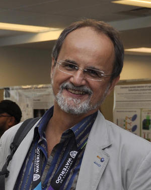 Zbigniew Wasilewski合作论文数Department of Physics and Astronomy, University of Waterloo3k korwinmikke合作论文数2z sidor合作论文数2G. Kamler合作论文数2
 Witold Rzodkiewicz合作论文数Glowny Urzad Miar, ul Elektoralna 2, PL-00139 Warsaw, Poland2
 Taube, A.合作论文数2Malachowski, T.合作论文数2Sobczak, G.合作论文数2
 Iwona Pasternak合作论文数Inst Elect Mat Technol2Gieraltowska Sylwia合作论文数1Institute of Physics, Polish Academy of Sciences2A. CZERWINSKI合作论文数2
 Rafał Jakieła合作论文数Laboratory of X-Ray and Electron Microscopy Research, Institute of Physics, Polish Academy of Sciences2Krzysztof Domanski合作论文数2




