Display Omitted We model thermo-mechanical stresses in silicon after annealing of TSVs.Results deliver detailed stress information of specific stress components.FEM demonstrates that the induced stress distribution is complex and cannot be described by a uniaxial stress thesis.Tensions decrease with increasing distance to the TSV.Simulation is validated by micro Raman spectroscopy measurements. In this paper thermo-mechanical stresses generated by TSV annealing are the center of interest. For this reason TSV die samples underwent annealing at 250¿C for 2h. In order to characterize the stress state after annealing µ-Raman spectroscopy (µRS) line scans were carried out subsequently using a 442nm laser. Then the respective spectra were fitted with a Lorentz function and the associated peak shifts were calculated. In general these results can be used to identify regions of mechanical tension. Unfortunately, µRS results do not allow any differentiation of the stress tensor components. Therefore a finite element model was developed to determine the stress tensor components after annealing. The FE-model was supplemented by a Matlab script, which converted stress data from simulation into Raman shifts using a general hypothesis. Further on physical aspects like penetration depth and laser spot size were taken into account. So the evaluation moved from single node results to a constrained section similar to the laser excited region in a µRS measurement. Proceeding this way allowed the adaption of FE results to µRS measurement properties. This enabled a bilateral validation of measurement and simulation.In summary our paper contributes valuable results for the TSV stress characterization and demonstrates further progress in µRS measurements in combination with FEM.
Crack propagation in BEoL (back-end of line) interconnect structures is a concern in terms of chip reliability. Due to the application of porous ultra low-k (ULK) materials, a careful trade-off is necessary between reducing signal delays and also decreasing mechanical properties of the interconnect structures. Therefore, fast and reliable measurement techniques for characterizing mechanical properties as film adhesion and fracture toughness are needed. In the present investigation, a camera assisted double-cantilever beam (DCB) technique has been used to obtain locally resolved adhesion measurements within the die. Two chip designs, produced in leading-edge technology nodes with two different ULK materials, were tested. The Gc values measured within the die show a correlation to density and arrangement of the Cu structures. ULK containing metallization levels with lowest k values have been identified as preferred crack paths. The measurements are compared with results of the four-point bending (4PB) test not having the local resolution of DCB but typically used for unpatterned film stacks and possessing a mode I/II load mixity. The DCB tests yield reduced Gc values compared to the 4PB tests, which can be understood as result of the different loading modes of both techniques.
For monitoring and improving mechanical properties of BEoL (back-end of line) interconnect structures in microprocessor technology, it is crucial to analyze their adhesion and crack propagation properties. In the present investigation, a camera assisted 4-point bending beam technique has been used to obtain fast and reliable adhesion measurements including locally resolved crack length information. To interpret the obtained crack propagation data, a finite-element modeling approach has been utilized. The combination of local measurement of the crack energy release rate and modeling enables to evaluate measurement curves for both symmetric and asymmetric crack propagation modes and to describe the crack propagation properties of the involved film stacks not attainable in such detail by conventional 4-point bending technique. (C) 2012 Elsevier Ltd. All rights reserved.
The magnetostriction of as-sputtered and annealed 400 nm thick Co films has been studied in longitudinal and transverse magnetic fields. The appreciable change of the magnetostriction behavior after annealing above 250 °C is correlated to grain growth and to the related change of the texture (from nearly randomly distributed hcp-Co crystallites to a c-axes texture perpendicular to the film plane). The magnetostriction behavior in the annealed samples cannot be explained by a domain magnetization within the film plane. It is assumed that a rotation of the spontaneous magnetization out of the film plane occurs due to the development of a perpendicular magnetic anisotropy.
In this paper, we present a novel micromachined Atomic Force Microscopy (AFM) micro-cantilever equipped with a sharp, conductive platinum tip. The processing sequence proposed in this article integrates a high reproducibility and precise post-processing applying Focused Ion Beam tip modification. The cantilever is designed for Scanning Thermal Microscopy (SThM) applications in a standard setup with the optical AFM detection system.
A force-sensor technique was developed to determine small forces in-situ in a scanning electron microscope (SEM), enabling to investigate elastic and plastic deformation modes and corresponding critical strains in single silicon lamellae. Large elastic deformations were obtained, matching with modeling of the Si deformation behavior by finite element analysis. This technique is shown to be applicable also to copper structures obtained after filling of the space between the Si lamellae and subsequent etching. The obtained mechanical properties of the structures on a nanoscale are important for the design of present and next-generation microprocessors.
Strained silicon underneath the field-effect transistor gate increases significantly the charge carrier mobility and thus improves the performance of leading-edge Complementary Metal Oxide Semiconductor (CMOS) devices For better understanding of the structure-strain relationship on the nanoscale and for optimization of device structures, the measurement of the local strain state has become essential Raman spectroscopy is used in the present investigation to analyze the strain distribution in and close to silicon/embedded silicon-germanium (SiGe) line structures in conjunction with strain modeling applying finite element analysis Both experimental results and modeling indicate the impact of geometry on the stress state An increase of compressive stress within the Si lines is obtained for increasing SiGe line widths and decreasing Si line widths The stress state within the Si lines is shown to be a mixed one deviating from a pure uniaxial state Underneath the SiGe cavities, the presence of a tensile stress was observed To investigate a procedure to scale down the spatial resolution of the Raman measurements, tip-enhanced Raman scattering experiments have been performed on free-standing SiGe lines with 100nm line width and line distance The results show superior resolution and strain information not attainable in conventional Raman scans
We have investigated silicon-germanium (SiGe) line structures employing metallic apertures in combination with Raman spectroscopy to obtain high-spatial strain resolution below the diffraction limit. The apertures were cut into specifically shaped electrochemically etched tungsten tips, which were adjusted within the Raman laser beam on the sample surface by a tuning fork atomic force microscope. With this setup, line structures on patterned SiGe films with a center-to-center distance down to 200 nm were resolved in the Raman scans, evidently indicating a resolution clearly below the far-field Raman resolution of about 600 nm for the used instrument. This setup allows improved local strain analysis by Raman spectroscopy and shows potential for further near-field Raman applications. Copyright (c) 2008 John Wiley & Sons, Ltd.
Raman intensity enhancement induced by nanoprobes (metal particles and metallised tips) approached to a strained silicon sample surface is reported. With silver nanoparticles deposited onto a silicon surface, high enhancements in the vicinity of particles were observed. Furthermore, metallised tips were scanned inside the spot of the laser used for Raman measurements. Both silver-coated and pure silver tips, mounted onto a tuning fork, indicated high Raman signal enhancement for optimised tip position within the laser spot. Atomic force microscopy was performed on a structured sample to investigate the stability of these tips. Focused ion beam was utilized to refine and to re-sharpen pure silver tips after the measurements. Complementary measurements were performed using pure tungsten tips. Due to the high hardness of W wires, a special pre-etching technique was applied in this case.
A promising approach to improve the performance of present CMOS devices is to introduce mechanical strain into the channel regions below the transistor gates. Strain can be generated as global strain on the whole wafer level (e.g., by growing strained silicon films on strain-relaxed silicon–germanium (SiGe) alloy layers or by using strained silicon films on an insulator), or as local strain on the transistor scale by applying specific technology processes (e.g., making use of embedded SiGe source-drain regions). The detection of strain in very thin silicon films requires sophisticated techniques with high depth sensitivity, whereas the measurement of the local strain state in thin Si structures with small lateral dimensions below 50 nm – such as the channels of current CMOS transistors – still remains to be mastered. A technique possessing the potential for solving this problem is Raman spectroscopy, where the diffraction limit for lateral resolution can be bypassed by near-field approaches. In the present paper, the occurrence of large strains in SiGe films and corresponding stresses in the GPa range are demonstrated by Raman spectroscopy, utilizing a simple approach for determining strain and composition separately. To estimate the strain distribution in a silicon channel structure due to embedded SiGe source–drain regions, a silicon strain calculation is applied based on a continuum-mechanical model utilizing a continuous distribution of virtual dislocations along the Si–SiGe boundaries. Within the framework of this model, the stress state in a 2D approximation is obtained by analytical expressions. Thus, the spatial distribution of channel strain and the impact of geometry on the strain state are obtained in a straightforward way.
Stresses in thin films can have important impact on microstructure, performance, and reliability in devices. Whereas sensitive stress determination in plane films is attainable by several methods like wafer‐curvature measurement or X‐ray diffraction, the latter is an appropriate tool also in structures with more complicated stress state. Subject of the present paper are stresses in arrays of parallel copper trench structures serving as model structure for interconnects in microelectronic devices. The stresses in such systems are important for device reliability, e.g. stability against electromigration, and mechanical stability in the dielectric environment, especially in case of low‐k dielectrics with the tendency of decreasing elastic constants. Stresses determined by the sin2 ψ‐technique are compared with model considerations based on Eshelby’s inclusion approximation approach, which allows straightforward modeling of the impact of trench geometry on the distribution of the internal stresses. The stress states obtained from different model assumptions are compared.
The effect of the nitrogen content on the thermal stability and degradation mechanisms of Ta–Si–N diffusion barriers was studied using methods that prove Cu interdiffusion. On the one hand, glancing angle X-ray diffraction was applied to detect Cu3Si formation after annealing of Cu/Ta–Si–N/Si layer stacks. On the other hand, a combined secondary ion mass spectroscopy and transmission electron microscopy analysis of Ta–Si–N/Cu/Ta–Si–N/SiO2/Si samples was performed. For a detailed investigation of the microstructure evolution, the crystallization behavior of both Cu-capped and uncapped Ta–Si–N/Si samples was analyzed using X-ray diffraction. In the case of an uncapped Ta73Si27 film, Si interdiffusion from the substrate precedes the layer crystallization. The substrate influence on the crystallization process decreases with increasing N content xN of the Ta–Si–N layer. Using Cu/Ta–Si–N/Si samples, a critical temperature for Cu silicide formation was determined. This temperature increases with increasing N content of the Ta–Si–N barrier. In the case of Ta–Si–N films with xN>25 at.%, Cu interdiffusion into the substrate occurs before a significant barrier crystallization is observed. For Ta–Si–N layers with xN≤25 at.%, no indications for Cu diffusion before crystalline phase formation were detected.
Resonant scattering with polarized X-ray radiation tuned to the Co L3 edge was employed to investigate structural and magnetic properties of Co/Cu multilayers showing giant magnetoresistance (GMR). The in-situ performed annealing up to 225°C lead to a reduction of the initially antiferromagnetic coupling of the Co layers and to an increasing ferromagnetic coupling contribution. The layer set-up persisted during annealing.
Soft X-ray magnetic reflection spectroscopy with linearly polarized light was used to investigate thin Fe films close to their 3p absorption edges. The high reflectivity in this spectral range enables one to measure magnetic signals in a wide angular range up to near-normal incidence. A strong amplification of the T-MOKE (transversal magneto-optical Kerr effect) asymmetry ratio occurs close to scattering angles of theta similar to 45 degrees and leads to huge magnetic signals of more than 50%. Utilizing these high signals, the course of the in-plane sample magnetization during the hysteresis cycle was determined from the variation of the hysteresis loops with the measurement geometry. (c) 2005 Elsevier B.V. All rights reserved.
Scattering of polarized soft x-rays is applied to study the magnetic and structural properties of Co/Cu GMR (giant magnetoresistance) layer stacks. The Co/Cu multilayers with layer thicknesses tuned to the second maximum of the GMR show a pronounced series of half-integer-order magnetic Bragg peaks in reflectometry curves measured at the Co L-2,L-3 absorption edges. These peaks of purely magnetic origin arise due to the antiparallel alignment of neighboring magnetic layers caused by interlayer exchange coupling. In applied magnetic fields the antiferromagnetic coupling is reduced, as proved by a reduction of the magnetic peaks in both specular and diffuse scattering. The magneto-optical constants at the Co L edges were determined from the energy dependence of the Bragg peak positions and utilized for modeling the scattering curves. Upon magnetization reversal, the reflectometry curves exhibit angular-dependent asymmetry effects, which indicate a high sensitivity of the magnetic signal on the probing depth. Comparison of x-ray magnetic hysteresis loops measured at the one-half and higher-order half-integer Bragg peaks shows that for detailed structural and magnetic information, the higher-order peaks have to be evaluated, too. Through the angular dependence of the hysteresis loops, they can be tuned to show antiferromagnetic and ferromagnetic features separately.
The magnetic coupling in Co/Cu multilayers with individual layer thicknesses tuned to the 2nd maximum of the giant magnetoresistance (GMR) is investigated by soft X-ray magnetic scattering. A series of half-integer order magnetic peaks appears in the specularly scattered intensity especially with the higher orders being strongly sensitive to magnetic effects. Diffuse magnetic scattering, performed with polarized neutrons, indicates long-range magnetic correlation in the remanent multilayer state and a corresponding magnetic domain structure sensitive to the magnetic field applied before.
 Claus Michael Schneider合作论文数Forschungszentrum Jülich29
 Norbert Mattern合作论文数Leibniz Institute for Solid State and Materials Research Dresden, Institute for Complex Materials15Ehrenfried Zschech合作论文数15HJ Engelmann合作论文数11
 Klaus Wetzig合作论文数10Volker Hoffmann合作论文数10
 Hans- Christoph Mertins合作论文数9René Hübner合作论文数9W. Brückner合作论文数9
 C. Wenzel合作论文数Semiconductor and Microsystems Laboratory, Dresden University of Technology9D Tietjen合作论文数8
 Ramona Ecke合作论文数7T. Gessner合作论文数6
 Zbigniew Celinski合作论文数Physics Department, Simon Fraser University6
 Jurgen Thomas合作论文数6
 Peter Oppeneer合作论文数Department of Physics and Astronomy, Uppsala University6
 Bob Camley合作论文数Department of Physics and Energy Science, College of Letters, Arts and Sciences, University of Colorado Colorado Springs5Y. Ritz合作论文数5
 Stefan Baunack合作论文数IFW Dresden5Se Schulz合作论文数4D. Abramsohn合作论文数4N. Cramer合作论文数4D. Elefant合作论文数4L. Van Loyen合作论文数4
 Sergio Valencia合作论文数Helmholtz Zentrum Berlin Mat & Energie4Leszek Malkinski合作论文数4
 Henning Heuer合作论文数IZFP Dresden Branch, Fraunhofer Institute for Non-Destructive Testing4
 Grzegorz Wielgoszewski合作论文数3
 Paweł Janus合作论文数3Dariusz Szmigiel合作论文数Institute of Electron Technology, Al. Lotników 32/46, 02-668 Warsaw, Poland3
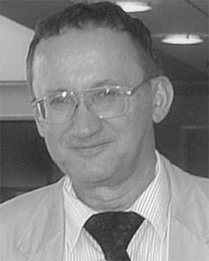 Piotr Grabiec合作论文数Instytut Technologii Elektronowej, Zakład Technologii Mikrosystemów i Nanostruktur Krzemowych, Aleja Lotników 32/46, 02-668 Warszawa, Poland3Przemyslaw Sulecki合作论文数3Joachim Schumann合作论文数3Teodor Gotszalk合作论文数Wroclaw University of Technology (WEMIF),3
 Horst Wendrock合作论文数3T O'Keevan合作论文数2U. Muschiol合作论文数2W Gudat合作论文数2S Menzel合作论文数2Dirk Fischer合作论文数2H. Geisler合作论文数2E Zschech合作论文数2Acker Jörg合作论文数2
 Franz Schafers合作论文数Department Optics and Beamlines, Helmholtz-Zentrum Berlin2J. He合作论文数2
 J. Szade合作论文数Institute of Physics, University of Silesia2An Qiu合作论文数2Rainer Kaltofen合作论文数2C.A. Kleint合作论文数2




