As GPUs scale their low-precision matrix math throughput to boost deep learning (DL) performance, they upset the balance between math throughput and memory system capabilities. We demonstrate that a converged GPU design trying to address diverging architectural requirements between FP32 (or larger)-based HPC and FP16 (or smaller)-based DL workloads results in sub-optimal configurations for either of the application domains. We argue that a C omposable O n- PA ckage GPU (COPA-GPU) architecture to provide domain-specialized GPU products is the most practical solution to these diverging requirements. A COPA-GPU leverages multi-chip-module disaggregation to support maximal design reuse, along with memory system specialization per application domain. We show how a COPA-GPU enables DL-specialized products by modular augmentation of the baseline GPU architecture with up to 4× higher off-die bandwidth, 32× larger on-package cache, and 2.3× higher DRAM bandwidth and capacity, while conveniently supporting scaled-down HPC-oriented designs. This work explores the microarchitectural design necessary to enable composable GPUs and evaluates the benefits composability can provide to HPC, DL training, and DL inference. We show that when compared to a converged GPU design, a DL-optimized COPA-GPU featuring a combination of 16× larger cache capacity and 1.6× higher DRAM bandwidth scales per-GPU training and inference performance by 31% and 35%, respectively, and reduces the number of GPU instances by 50% in scale-out training scenarios.
Pulse Amplitude Modulation (PAM) uses multiple voltage levels as different data symbols, transferring multiple bits of data simultaneously, thereby enabling higher communication bandwidth without increased operating frequencies. However, dividing the voltage into more symbols leads to a smaller voltage difference between adjacent symbols, making the interface more vulnerable to crosstalk and power noise. GDDR6X adopts four-level symbols (PAM4) with Maximum Transition Avoidance (MTA) coding, which reduces the effects of crosstalk. However, current coding approaches can consume excess energy and produce excess power noise. This paper introduces novel energy reduction techniques for PAM interfaces, specifically demonstrating them for GDDR6X PAM4. Inspired by prior work on conventional single-ended I/O interfaces, we leverage the unused idle periods in DRAM channels between data transmissions to apply longer but more energy-efficient codes. To maximize the energy savings, we build multiple sparse encoding schemes to fit different sized gaps in the DRAM traffic. These sparse encodings can provide energy reductions of up to 52% when transferring 4-bit data using a 3-symbol sequence. We evaluate these coding techniques using an NVIDIA RTX 3090 baseline, a recent GPU which uses GDDR6X with PAM4 signaling. Our evaluation shows the opportunity for large energy savings at the DRAM I/O interface (28.2% on average) over many HPC/DL applications with minimal performance degradation.
Achieving peak performance on sparse operations is challenging. The distribution of the non-zero elements and underlying hardware platform affect the execution efficiency. Given the diversity in workloads and architectures, no unique solution always wins. In this paper, we improve SpMM efficiency on GPUs. We propose several simple, but effective, sparse data permutations on the CSR data structure. Picking the right permutation over 1,688 datasets improves performance by 1.4×, on average, compared to plain CSR and 2.6× against NVIDIA cuSPARSE. Furthermore, we propose a set of novel features to describe sparsity patterns and their interactions with the kernel and hardware. Using these features, we develop a predictor to select the best permutation for each matrix. Predicted permutations' average gain achieves 96% of oracle gains.
The demands of high-performance computing (HPC) and machine learning (ML) workloads have resulted in the rapid architectural evolution of GPUs over the last decade. The growing memory footprint and diversity of data types in these workloads has required GPUs to embrace micro-architectural heterogeneity and increased memory system sophistication to scale performance. Effective simulation of new architectural features early in the design cycle enables quick and effective exploration of design trade-offs across this increasingly diverse set of workloads. This work provides a retrospective on the design and development of NVArchSim (NVAS), an architectural simulator used within NVIDIA to design and evaluate features that are difficult to appraise using other methodologies due to workload type, size, complexity, or lack of modeling flexibility. We argue that overly precise and/or overly slow architectural models hamper an architect's ability to evaluate new features within a reasonable time frame, hurting productivity. Because of its speed, NVAS is being used to trace and evaluate hundreds of HPC and state-of-the-art ML workloads on single-GPU or multi-GPU systems. By adding component fidelity only when necessary to improve system-level modeling accuracy, NVAS delivers simulation speed orders of magnitude higher than most publicly available GPU simulators while retaining high levels of accuracy and simulation flexibility. Building trustworthy high-level simulation platforms is a difficult exercise in balance and compromise; we share our experiences to help and encourage those in academia who take on the challenge of building GPU simulation platforms.
Efficient manipulation of sparse matrices is critical to a wide range of HPC applications. Increasingly, GPUs are used to accelerate these sparse matrix operations. We study one common operation, Sparse Matrix Multi-Vector Multiplication (SpMM), and evaluate the impact of the sparsity, distribution of non-zero elements, and tiletraversal strategies on GPU implementations. Using these insights, we determine that operating on these sparse matrices in a Densified Compressed Sparse Row (DCSR) is well-suited to the parallel warp-synchronous execution model of the GPU processing elements. Preprocessing or storing the sparse matrix in the DCSR format, however, often requires significantly more memory storage than conventional Compressed Sparse Row (CSR) or Compressed Sparse Column (CSC) formats. Given that SpMM kernels are often bottlenecked on DRAM bandwidth, the increase in DRAM traffic to access the larger DCSR formatted data structure can result in a slowdown for many matrices. We propose a near-memory transform engine to dynamically create DCSR formatted tiles for the GPU processing elements from the CSC formatted matrix in memory. This work enhances a GPU's last-level cache/memory controller unit to act as an efficient translator between the compute-optimized representation of data and its corresponding storage/bandwidth-optimized format to accelerate sparse workloads. Our approach achieves 2.26x better performance on average compared to the vendor supplied optimized library for sparse matrix operations, cuSPARSE.
Training convolutional neural networks (CNNs) requires intense compute throughput and high memory bandwidth. Especially, convolution layers account for the majority of execution time of CNN training, and GPUs are commonly used to accelerate these layer workloads. GPU design optimization for efficient CNN training acceleration requires the accurate modeling of how their performance improves when computing and memory resources are increased. We present DeLTA, the first analytical model that accurately estimates the traffic at each GPU memory hierarchy level, while accounting for the complex reuse patterns of a parallel convolution algorithm. We demonstrate that our model is both accurate and robust for different CNNs and GPU architectures. We then show how this model can be used to carefully balance the scaling of different GPU resources for efficient CNN performance improvement.
Popular deep learning frameworks require users to fine-tune their memory usage so that the training data of a deep neural network (DNN) fits within the GPU physical memory. Prior work tries to address this restriction by virtualizing the memory usage of DNNs, enabling both CPU and GPU memory to be utilized for memory allocations. Despite its merits, virtualizing memory can incur significant performance overheads when the time needed to copy data back and forth from CPU memory is higher than the latency to perform DNN computations. We introduce a high-performance virtualization strategy based on a "compressing DMA engine" (cDMA) that drastically reduces the size of the data structures that are targeted for CPU-side allocations. The cDMA engine offers an average 2.6x (maximum 13.8x) compression ratio by exploiting the sparsity inherent in offloaded data, improving the performance of virtualized DNNs by an average 53% (maximum 79%) when evaluated on an NVIDIA Titan Xp.
Main memory (DRAM) consumes as much as half of the total system power in a computer today, due to the increasing demand for memory capacity and bandwidth. There is a growing need to understand and analyze DRAM power consumption, which can be used to research new DRAM architectures and systems that consume less power. A major obstacle against such research is the lack of detailed and accurate information on the power consumption behavior of modern DRAM devices. Researchers have long relied on DRAM power models that are predominantly based off of a set of standardized current measurements provided by DRAM vendors, called IDD values. Unfortunately, we find that state-of-the-art DRAM power models are often highly inaccurate when compared with the real power consumed by DRAM. This is because existing DRAM power models (1) are based off of the worst-case power consumption of devices, as vendor specifications list the current consumed by the most power-hungry device sold; (2) do not capture variations in DRAM power consumption due to different data value patterns; and (3) do not account for any variation across different devices or within a device.
This paper summarizes our work on experimental characterization and analysis of reduced-voltage operation in modern DRAM chips, which was published in SIGMETRICS 2017, and examines the work's significance and future potential. We take a comprehensive approach to understanding and exploiting the latency and reliability characteristics of modern DRAM when the DRAM supply voltage is lowered below the nominal voltage level specified by DRAM standards. We perform an experimental study of 124 real DDR3L (low-voltage) DRAM chips manufactured recently by three major DRAM vendors. We find that reducing the supply voltage below a certain point introduces bit errors in the data, and we comprehensively characterize the behavior of these errors. We discover that these errors can be avoided by increasing the latency of three major DRAM operations (activation, restoration, and precharge). We perform detailed DRAM circuit simulations to validate and explain our experimental findings. We also characterize the various relationships between reduced supply voltage and error locations, stored data patterns, DRAM temperature, and data retention. Based on our observations, we propose a new DRAM energy reduction mechanism, called Voltron. The key idea of Voltron is to use a performance model to determine by how much we can reduce the supply voltage without introducing errors and without exceeding a user-specified threshold for performance loss. Our evaluations show that Voltron reduces the average DRAM and system energy consumption by 10.5% and 7.3%, respectively, while limiting the average system performance loss to only 1.8%, for a variety of memory-intensive quad-core workloads. We also show that Voltron significantly outperforms prior dynamic voltage and frequency scaling mechanisms for DRAM.
Modern highly parallel GPU systems require highbandwidth DRAM I/O interfaces that can consume a significant amount of energy. This energy increases in proportion to the number of 1 values in the data transactions due to the asymmetric energy consumption of Pseudo Open Drain (POD) I/O interface in contemporary Graphics DDR SDRAMs. In this work, we describe a technique to save energy by reducing the energy-expensive 1 values in the DRAM interface. We observe that multiple data elements within a single cache line/sector are often similar to one another. We exploit this characteristic to encode each transfer to the DRAM such that there is one reference copy of the data, with remaining similar data items being encoded predominantly as 0 values. Our proposed low energy data transfer mechanism, Base+XOR Transfer, encodes the data-similar portion by performing XOR operations between data elements within a single DRAM transaction. We address two challenges that influence the efficiency of our mechanism, i) the frequent appearance of zero data elements in transactions, and ii) the diversity in the underlying size of data types within a transaction. We describe two techniques, Zero Data Remapping and Universal Base+XOR Transfer, to efficiently address these issues. Our proposed encoding scheme requires no additional metadata or changes to existing DRAM devices. We evaluate our mechanism on a modern high performance GPU system with a variety of graphics and compute workloads. We show that our mechanism reduces energy-expensive 1 values by 35.3% with minimal overheads, and combining our mechanism with Dynamic Bus Inversion (DBI) reduces 1 values by 48.2% on average. These 1 value reductions lead to 5.8% and 7.1% DRAM energy savings, respectively.
This paper proposes an energy-efficient, high-throughput DRAM architecture for GPUs and throughput processors. In these systems, requests from thousands of concurrent threads compete for a limited number of DRAM row buffers. As a result, only a fraction of the data fetched into a row buffer is used, leading to significant energy overheads. Our proposed DRAM architecture exploits the hierarchical organization of a DRAM bank to reduce the minimum row activation granularity. To avoid significant incremental area with this approach, we must partition the DRAM datapath into a number of semi-independent subchannels. These narrow subchannels increase data toggling energy which we mitigate using a static data reordering scheme designed to lower the toggle rate. This design has 35% lower energy consumption than a die-stacked DRAM with 2.6% area overhead. The resulting architecture, when augmented with an improved memory access protocol, can support parallel operations across the semi-independent subchannels, thereby improving system performance by 13% on average for a range of workloads.
3D-stacked memory devices with processing logic can help alleviate the memory bandwidth bottleneck in GPUs. However, in order for such Near-Data Processing (NDP) memory stacks to be used for different GPU architectures, it is desirable to standardize the NDP architecture. Our proposal enables this standardization by allowing data to be spread across multiple memory stacks as is the norm in high-performance systems without an MMU on the NDP stack. The keys to this architecture are the ability to move data between memory stacks as required for computation, and a partitioned execution mechanism that offloads memory-intensive application segments onto the NDP stack and decouples address translation from DRAM accesses. By enhancing this system with a smart offload selection mechanism that is cognizant of the compute capability of the NDP and cache locality on the host processor, system performance and energy are improved by up to 66.8% and 37.6%, respectively.
The energy consumption of DRAM is a critical concern in modern computing systems. Improvements in manufacturing process technology have allowed DRAM vendors to lower the DRAM supply voltage conservatively, which reduces some of the DRAM energy consumption. We would like to reduce the DRAM supply voltage more aggressively, to further reduce energy. Aggressive supply voltage reduction requires a thorough understanding of the effect voltage scaling has on DRAM access latency and DRAM reliability. In this paper, we take a comprehensive approach to understanding and exploiting the latency and reliability characteristics of modern DRAM when the supply voltage is lowered below the nominal voltage level specified by manufacturers.
Future GPUs and other high-performance throughput processors will require multiple TB/s of bandwidth to DRAM. Satisfying this bandwidth demand within an acceptable energy budget is a challenge in these extreme bandwidth memory systems. We propose a new high-bandwidth DRAM architecture, Fine-Grained DRAM (FGDRAM), which improves bandwidth by 4× and improves the energy efficiency of DRAM by 2× relative to the highest-bandwidth, most energy-efficient contemporary DRAM, High Bandwidth Memory (HBM2). These benefits are in large measure achieved by partitioning the DRAM die into many independent units, called grains, each of which has a local, adjacent I/O. This approach unlocks the bandwidth of all the banks in the DRAM to be used simultaneously, eliminating shared buses interconnecting various banks. Furthermore, the on-DRAM data movement energy is significantly reduced due to the much shorter wiring distance between the cell array and the local I/O. This FGDRAM architecture readily lends itself to leveraging existing techniques to reducing the effective DRAM row size in an area efficient manner, reducing wasteful row activate energy in applications with low locality. In addition, when FGDRAM is paired with a memory controller optimized to exploit the additional concurrency provided by the independent grains, it improves GPU system performance by 19% over an iso-bandwidth and iso-capacity future HBM baseline. Thus, this energy-efficient, high-bandwidth FGDRAM architecture addresses the needs of future extreme-bandwidth memory systems. CCS CONCEPTS • Hardware → Dynamic memory; Power and energy; • Computing methodologies → Graphics processors; • Computer systems organization → Parallel architectures;
The energy consumption of DRAM is a critical concern in modern computing systems. Improvements in manufacturing process technology have allowed DRAM vendors to lower the DRAM supply voltage conservatively, which reduces some of the DRAM energy consumption. We would like to reduce the DRAM supply voltage more aggressively, to further reduce energy. Aggressive supply voltage reduction requires a thorough understanding of the effect voltage scaling has on DRAM access latency and DRAM reliability. In this paper, we take a comprehensive approach to understanding and exploiting the latency and reliability characteristics of modern DRAM when the supply voltage is lowered below the nominal voltage level specified by DRAM standards. Using an FPGA-based testing platform, we perform an experimental study of 124 real DDR3L (low-voltage) DRAM chips manufactured recently by three major DRAM vendors. We find that reducing the supply voltage below a certain point introduces bit errors in the data, and we comprehensively characterize the behavior of these errors. We discover that these errors can be avoided by increasing the latency of three major DRAM operations (activation, restoration, and precharge). We perform detailed DRAM circuit simulations to validate and explain our experimental findings. We also characterize the various relationships between reduced supply voltage and error locations, stored data patterns, DRAM temperature, and data retention. Based on our observations, we propose a new DRAM energy reduction mechanism, called Voltron. The key idea of Voltron is to use a performance model to determine by how much we can reduce the supply voltage without introducing errors and without exceeding a user-specified threshold for performance loss. Our evaluations show that Voltron reduces the average DRAM and system energy consumption by 10.5% and 7.3%, respectively, while limiting the average system performance loss to only 1.8%, for a variety of memory-intensive quad-core workloads. We also show that Voltron significantly outperforms prior dynamic voltage and frequency scaling mechanisms for DRAM.
Main memory bandwidth is a critical bottleneck for modern GPU systems due to limited off-chip pin bandwidth. 3D-stacked memory architectures provide a promising opportunity to significantly alleviate this bottleneck by directly connecting a logic layer to the DRAM layers with high bandwidth connections. Recent work has shown promising potential performance benefits from an architecture that connects multiple such 3D-stacked memories and offloads bandwidth-intensive computations to a GPU in each of the logic layers. An unsolved key challenge in such a system is how to enable computation offloading and data mapping to multiple 3D-stacked memories without burdening the programmer such that any application can transparently benefit from near-data processing capabilities in the logic layer. Our paper develops two new mechanisms to address this key challenge. First, a compiler-based technique that automatically identifies code to offload to a logic-layer GPU based on a simple cost-benefit analysis. Second, a software/hardware cooperative mechanism that predicts which memory pages will be accessed by offloaded code, and places those pages in the memory stack closest to the offloaded code, to minimize off-chip bandwidth consumption. We call the combination of these two programmer-transparent mechanisms TOM: Transparent Offloading and Mapping. Our extensive evaluations across a variety of modern memory-intensive GPU workloads show that, without requiring any program modification, TOM significantly improves performance (by 30% on average, and up to 76%) compared to a baseline GPU system that cannot offload computation to 3D-stacked memories.
In future memory systems, some regions of memory will be periodically unavailable to the processor. In DRAM systems, this may happen because a rank is busy performing refresh. In non-volatile memory systems, this may happen because a rank is busy draining long-latency writes. Unfortunately, such service interruptions can introduce stalls in all running threads. This is because the operating system spreads the pages of a thread across all memory ranks. Therefore, the probability of a thread accessing data in an unavailable rank is high. This is a performance artifact that has previously not been carefully analyzed. To reduce these stalls, we propose a simple page coloring mechanism that tries to minimize the number of ranks over which a thread's pages are spread. This approach ensures that a service interruption in a single rank only stalls a subset of threads; non-stalled threads even have the potential to run faster at this time because of reduced bus contention. Our analysis shows that this approach is more effective than recent hardware-based mechanisms to deal with such service interruptions. For example, when dealing with service interruptions because of DRAM refresh, the proposed page coloring approach yields an execution time that is 15% lower than the best competing hardware approach.
With increasing DRAM densities, the performance and energy overheads of refresh operations are increasingly significant. When the system is active, refresh commands render DRAM banks unavailable for increasing periods of time. These refresh operations can interfere with regular memory operations and hurt performance. In addition, when the system is idle, DRAM self-refresh is the dominant source of energy consumption, and it directly impacts battery life and standby time. Prior refresh reduction techniques seek to reduce active-mode auto-refresh energy, reduce self-refresh energy, improve performance, or some combination thereof. In this paper, we present CLARA, a circular linked-list based refresh architecture which meets all three goals with very low overheads and without sacrificing DRAM capacity. This approach exploits the variation in retention time at a chip granularity as opposed to a DIMM-wide, rank granularity in prior work. CLARA reduces auto- and self-refresh by 86.2%, independent of workload. Auto refresh reduction improves average CPU performance by 3.1% and 6.5% in the normal and extended temperature range, respectively. GPU performance improves by 2.1% on average in the extended temperature range. DRAM idle power during self-refresh is reduced by 44%. The area overhead of CLARA in the DRAM is about 0.085% and negligible in the memory controller.
 Mike O'Connor合作论文数NVIDIA16
 Rajeev Balasubramonian合作论文数School of Computing, University of Utah15
 Donghyuk Lee合作论文数NVIDIA11
 Stephen W. Keckler合作论文数Nvidia8
 Onur Mutlu合作论文数Department of Information Technology and Electrical Engineering, Eidgenössische Technische Hochschule Zürich;Department of Electrical and Computer Engineering, College of Engineering, Carnegie Mellon University;Department of Computer Engineering, Bilkent University6
 Al Davis合作论文数Computer Science Department
University of Utah6
Al Davis合作论文数Computer Science Department
University of Utah6 Aditya Agrawal合作论文数ISIS, Vanderbilt University6
 Gabriel H. Loh合作论文数Advanced Micro Devices, Inc.5
 Manjunath Shevgoor合作论文数University of Utah5Nuwan Jayasena合作论文数Advanced Micro Devices5Aniruddha N. Udipi合作论文数University of Utah5james m oconnor合作论文数4Kevin Chang合作论文数4
 Abdullah Giray Yağlıkçı合作论文数Secure and Sustainable System Scaling Lab, CISPA Helmholtz Center for Information Security4
 Hasan Hassan合作论文数Meta4
 Norm Jouppi合作论文数Google4
 Saugata Ghose合作论文数Department of Computer Science, University of Illinois Urbana-Champaign;Siebel School of Computing and Data Science, The Grainger College of Engineering, University of Illinois Urbana-Champaign4
 Evgeny Bolotin合作论文数Electrical Engineering Department;Israel Institute of Technology;Electrical Engineering Department, Israel Institute of Technology4
 Naveen Muralimanohar合作论文数Google4
 Jung-Sik Kim合作论文数Kwangwoon University, Kwangwoon Univ3Seth H. Pugsley合作论文数Intel Labs, Hillsboro, OR, USA3
 David Nellans合作论文数NVIDIA3
 Benjamin C. Lee合作论文数Electrical and Computer Engineering Pratt School of Engineering Duke University3
 Abhijith Kashyap合作论文数University of California at Riverside3
 Minsoo Rhu合作论文数School of Electrical Engineering, Korea Advanced Institute of Science and Technology3alan lynn davis合作论文数2
 Kevin Hsieh合作论文数Microsoft2Yaosheng Fu合作论文数2
 Ali Shafiee Ardestani合作论文数Samsung Semiconductor Inc.;Meta Inc.2
 Chita R. Das合作论文数High Performance Computing Laboratory, Department of Computer Science and Engineering, School of Electrical Engineering and Computer Science, College of Engineering, Pennsylvania State University2
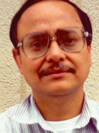 Pradip Bose合作论文数Department of Computer Science, IBM T.J. Watson Research Center2
 William J. Dally合作论文数NVIDIA;Computer Science Department, Stanford University2
 Alaa R. Alameldeen合作论文数School of Computing Science, Simon Fraser University2
 Mike Ferdman合作论文数Department of Computer Science, Stony Brook University;Telinta, Inc.2
 Adwait Jog合作论文数Department of Computer Science, School of Engineering and Applied Science, University of Virginia2
 Manu Awasthi合作论文数School of Computing;University of Utah;School of Computing, University of Utah2
 Gwangsun Kim合作论文数KAIST2Raghav Gupta合作论文数1
 Andrew Richard Putnam合作论文数1Kais Kudrolli合作论文数1Jun Yang合作论文数1
 Daichi Fujiki (藤木大地)合作论文数Institute of Integrated Research, Institute of Science Tokyo1Zi Yan合作论文数Department of Computer Science, Rutgers University1
 Ashutosh Pattnaik合作论文数Penn State Univ, University Pk, PA 16802 USA1
 Atefeh Mehrabi合作论文数Duke University1
 Youngeun Kwon合作论文数NVIDIA1Elvira Teran合作论文数Texas A&M University, College Station, TX, USA1
 Dmitry Ponomarev合作论文数VA Steklov Math Inst, RAS1
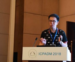 Guangyu Sun合作论文数State Key Lab Elect Insulat & Power Equipment, Xi An Jiao Tong Univ1




