3D NAND is one of the most promising storage devices due to its high storage density and low energy consumption. Selective wet etching of Si3N4 by hot-concentrated phosphoric acid (PA) solution is a key process for 3D NAND fabrication. However, the channel material, polycrystalline silicon (poly-Si), is unexpectedly dissolved due to its inevitable exposure to the PA etching solution, which causes device failure and thus limits the stacking density of 3D NAND. Herein, to avoid the detrimental dissolution of poly-Si, we unveil the mechanism of poly-Si dissolution in PA solution from kinetic and thermodynamic perspectives. We find that the etch process shows a two-stage reaction, in which H2O plays a key role in lowering the activation barrier for poly-Si etching. Further thermodynamic analysis demonstrates that poly-Si prefers to be oxidized by H2O to suboxide rather than to SiO2. Combined with surface chemistry characterization, we propose the dissolution mechanism as a two-stage process involving the dissolution of suboxide interface and bulk poly-Si, where the nucleophilic substitution of Si–H with Si–OH on bulk poly-Si surface determines the overall etch rate. This study advances the 3D NAND development by establishing a theoretical foundation for identifying and implementing efficacious strategies to impede detrimental dissolution.
The SiO2 layers, as the dielectric in the multistack storage cells of 3D NAND, are detrimentally dissolved by phosphoric acid (PA) during the selective Si3N4 etching. The thinning of SiO2 layers leads to the failure of subsequent processes; thus, an etching inhibitor for SiO2 is crucial for 3D NAND fabrication. However, most inhibitors are currently limited to neutral or alkaline solutions. In this work, the gamma-ureidopropyltriethoxysilane (UPTES), compatible with a hot-concentrated PA solution, was applied to the wet-etching process for the first time and exhibited an inhibitory effect on SiO2 etching by retarding the etch rate over 60% without affecting the Si3N4 etching. The saturation adsorption of UPTES on the SiO2 substrate is confirmed to occur around the critical concentration, according to the Langmuir-Freundlich adsorption isotherm. The adsorption behavior of UPTES exhibits a reliance on its concentration. Around the critical concentration, the UPTES molecules chemisorb on the SiO2 surface by Si-O-Si covalent bonds to form ordered UPTES-siloxane layers, avoiding contact between SiO2 and the etchant; whereas oversaturated UPTES polymers physisorb not only on SiO2 but also on Si3N4, impeding the Si3N4 etching. This work contributes to a step forward in the effective wet-etching process in high-density 3D NAND fabrication.
分别采用聚醚胺类物质、聚乙烯亚胺类物质和聚酰胺类物质作为大马士革铜互连电镀工艺的整平剂,得到杂质含量不同的Cu膜层,通过计时电位测试分析了不同整平剂对膜层杂质含量的影响机制.研究了杂质含量对Cu膜层自退火速率、应力和电阻率的影响.结果表明,膜层中杂质含量过高会引起Cu膜层的电阻和应力升高.采用聚乙烯亚胺类物质或聚酰胺类物质作为整平剂时电镀所得Cu膜层的杂质含量都较低.
3D NAND flash memory with vertically stacked cells has been developed to break through the limits of technology nodes. However, during the selective etching process, it is difficult to ensure the byproducts diffuse away from the trenches in the multistacked layers. Once saturated, the byproduct causes abnormal redeposition on the SiO2 layers. This problem has restricted the development of high-density 3D NAND memory. To solve this problem, the composition and formation mechanism of the redeposited layer must be clarified. In this study, a ternary-wafer system comprising a Si3N4/SiO2/Si3N4 stack was fabricated to study the redeposition mechanism, and the morphology, elastic properties, and chemical composition of the redeposited layer were clarified. The redeposited layer consists of spherical particles with elastic surfaces (average Young’s modulus of 24.17 GPa). The particles were confirmed to comprise colloidal silica gel covered by silanols. By considering the chemistry of silica, the redeposition mechanism was proposed as follows: colloidal silica gel is formed by the aggregation of silicic acids from Si3N4 etching, which adsorb onto the SiO2 layer through oxide bridges and hydrogen bonding. Our work will contribute to the development of high-density 3D NAND memory.
3D NAND has become one of the most promising storage devices to meet the growing demand for large-capacity data storage. Stacking more Si 3 N 4 /SiO 2 layers in 3D NAND is essential for increasing its storage density. However, as the number of stacked layers increased, technical difficulties including poor etch selectivity, redeposition on SiO 2 layers, and dissolution of poly-Si channel arise in the wet etching process of 3D NAND manufacturing, seriously damaging the performance and reliability of the device. In this paper, we studied the kinetic effects of fluorine- and silane-containing additives on Si 3 N 4 and SiO 2 etching. The additives affected the etch rates of Si 3 N 4 and SiO 2 by changing the activation energies, thereby adjusting the etch selectivity. Additionally, the redeposited colloidal silica gel on SiO 2 layers and the detrimental dissolution of poly-Si channel were characterized. These results will contribute to exploring solutions for challenges in 3D NAND manufacturing.
芯片中的钴互连作为铜互连之后的下一代互连技术受到了业界的极大关注,且已经引入集成电路7nm以下的制程.钴互连主要采用湿法的电化学沉积技术,但由于保密原因和研究条件的限制,其研究报道不多.本文基于现有专利、文献报道较系统地介绍了钴互连技术的优势及发展现状,并从溶液化学和电化学角度综述了钴互连电镀基本工艺、基础镀液组成与添加剂、超填充电镀机理,以及镀层退火控制与杂质影响等的研究现状,并对钴互连技术下一步研究进行了展望.
作为半导体市场中主要存储芯片之一,NAND已从2D发展到3D.3D NAND的立体存储结构提高了芯片容量、性能和可靠性.在3D NAND的交替堆栈结构中,需通过氮化-物氧化物的选择性刻蚀获得层间介质层,堆栈层数越多,芯片性能越好,但高层堆栈的刻蚀均匀性也更难保持,此时易出现SiO2在氧化层端头再沉积的回沾现象,层间结构被破坏,影响器件性能.要达到更高层数必须减少回沾,探究该过程及其影响因素成为关键所在.本文综述了3D NAND制程中氮化硅选择性刻蚀工艺的发展现状和现有研究成果,强调了控制硅含量对防止回沾的重要性,介绍了相关理论模型,提供模拟预测.为深入分析其中的化学反应,本文对相关的SiO2溶液化学进行了概述,总结了聚硅酸形成的影响因素,强调胶凝曲线能反应其聚合行为,据此可研究怎样通过影响硅酸聚合行为或聚硅酸在氧化层表面的沉积行为来防止回沾,以对未来研究起到理论指导作用.
Chemical mechanical polishing (CMP) performance influence the reliability of TSV process, because the wafer chip-to-chip vertical interconnections for the next process request the TSV wafer a flat surface without defects after CMP. The influence of ECD process to the CMP defects, further to the via-filling effect, was investigated. Thickness uniformity, top surface morphology and the grain orientation of the copper-filled via prove to be the major factors that lead to the CMP defects: Cu residue, delamination and pits. Optimizing the additives of ECD bath is proved to be a solution to eliminate the CMP defects.
A micro-compression test method was presented to evaluate the mechanical property of the TSV-Cu micropillar in this paper. Firstly, the test sample containing TSV-Cu micropillar was prepared by MEMS micromachining technology. Then, the mechanical property of TSV-Cu micropillar was measured by a self-made micro-compression system. Finally, the effect of thermal treatment on the mechanical property of TSV-Cu micropillar was studied. The experimental results showed that the average yield strength ( σ 0.2 ) of the TSV-Cu micropillar was 167 MPa. But it decreased to 137 MPa after being thermally treated at 400°C for 1 hour, which was probably due to the increased grain size of Cu.
使用Fluent流场仿真软件模拟了电镀液对硅通孔(TSV)的浸润过程,讨论了TSV深宽比、电镀液流速、电镀液表面张力、接触角以及压强等因素对TSV浸润过程的影响.通过对比仿真寻找出能在电镀之前使电镀液完全浸润TSV所有表面的预润湿处理方法,以防止因润湿不彻底在TSV底部形成气泡而导致的有空洞电镀填充.通过仿真发现,电镀液表面张力越小,电镀液与待电镀样片表面的接触角越小,浸润过程中电镀液的流速越慢,浸润所处环境的压强越低,则越有利于电镀液对TSV的浸润;且流速为0.002m/s时即可对深宽比低于或等于130 μm∶30μm的TSV实现完全浸润;浸润环境压强低于3 000 Pa时即可在流速为0.05 m/s时对深宽比为150 μm∶50 μm的TSV基本实现完全浸润.当TSV结构的深宽比大于2的时候,没有经过预润湿而直接放入电镀液的TSV结构很难实现无空洞电镀填充.
The Cu specimens were fabricated by the UV-LIGA process using the electrodeposition bath for through-silicon-via (TSV) filling. Mechanical properties of the Cu specimens annealed at different temperatures were investigated by a uniaxial tensile test. The results indicated that the yield strength and breaking strength of as-deposited Cu specimens were higher than that of the bulk Cu, while the elastic modulus was lower than that of the bulk Cu. The elastic modulus, yield strength and breaking strength of Cu specimens decreased with the increase of the annealing temperature. When the annealing temperature was 400^oC, the elastic modulus decreased from 95 to 69GPa, the yield strength decreased from 314 to 202MPa, and the breaking strength decreased from 367 to 290MPa, respectively. In contrast, the ultimate strain increased with increasing the annealing temperature. The surface morphology, fractography and crystal structure of the Cu specimens were characterized by SEM, TEM and XRD methods. The results indicated that the particle size increased with the increase of the annealing temperature, which contributed to the decrease of the yield strength and breaking strength according to the Hall-Petch law. The XRD results indicated that as-deposited Cu specimens had a preferred orientation in (220) plane, but (311) plane became the preferred orientation with increasing the temperature. This probably contributed to the decrease of the elastic modulus with increasing the temperature.
The Cu specimens were fabricated by the UV-LIGA process using the electrodeposition bath for through-silicon-via (TSV) filling. Mechanical property of th e Cu specimens was investigated by a uniaxial tensile test. The elastic modulus, yield strength, breaking stre ngth and ultimate strain are 95GPa, 314MPa, 367MPa and 12.4%, respectively. The results indicated that the yield strength and breaking strength of as-deposited Cu specimens were higher than that of the bulk Cu, while the elastic modulus was lower than that of the bulk Cu. The elastic modulus of C u thin film in surface and section are 115.7GPa and 105.4GPa measured by nanoindentation, respectively. This difference is caused by the difference of the grain orientation between the surface and section of Cu thin film.
Through silicon via (TSV) with many advantages comparing with traditional technology is playing an important role in three-dimensional large-scale integration. In this paper, we have studied Effect of leveler on microstructure and stress of electroplated copper for TSV application. We demonstrate residual stress, SEM, TEM and electrochemistry results which have strong connection with leveler in via copper electroplating solution.
The miniaturization trend of microelectric products gives birth to 3D stacking of chips, which is realized by using TSV (through silicon via) technique. A novel micro-tensile specimen of the uniaxial micro-tensile test for measuring the mechanical properties of Cu-TSV is proposed. Finite-Element Method (FEM) has been used to optimize the design of the supporting frame of the sample with a Cu-TSV thin film, which can effectively reduce the damage ratio of the sample during operations. The surface-treated Ti seed layer has substituted for the traditional Cr/Cu seed layer to reduce the stress concentration and prevent the specimen from alkali corrosion when etching the seed layer. The samples have been tested by the uniaxial micro-tensile system to obtain the mechanical properties of the Cu-TSV thin film. The measured Young's modulus and the ultimate tensile strength of Cu-TSV is 25.4--32. 9 GPa and 574--764 MPa, respectively.
 Zihan Zhou合作论文数6
 Yunwen Wu (吴蕴雯)合作论文数Institute of Electronic Materials and Technology, School of Materials Science and Engineering, Shanghai Jiao Tong University5
 Ming Li (李明)合作论文数School of Materials Science and Engineering, Shanghai Jiao Tong University5
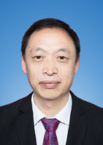 Guifu Ding (丁桂甫)合作论文数Department of Micro/Nano Electronic, School of Electronic Information and Electrical Engineering, Shanghai Jiao Tong University5
 Jie Guo合作论文数4Huiying Wang合作论文数4
 Ling Huiqin (凌惠琴)合作论文数School of Materials Science and Engineering, Shanghai Jiaotong University4Sihan Lin合作论文数3ting gu合作论文数3
 Tao Hang (杭弢)合作论文数School of Materials Science and Engineering, Shanghai Jiao Tong University3
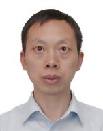 Hong Wang (王红)合作论文数School of Chemistry and Chemical Engineering, Shanghai Jiao Tong University3程萍合作论文数2Yu Xianxian合作论文数2
 Ping Cheng (郑平)合作论文数School of Mechanical Engineering, Shanghai Jiao Tong University2xiao lin zhao合作论文数1Chuang Jiang合作论文数1Yang Yuan合作论文数1ZHANG Zhen-jie (张振杰)合作论文数1heng yue (岳恒)合作论文数1Hong-qi SUN (孙红旗)合作论文数1
 Yan Wang (王艳)合作论文数Shanghai Jiao Tong University School of Medicine1Xue Feng合作论文数1
 Zhaoyu Wang合作论文数1
 Xiao Gu合作论文数1
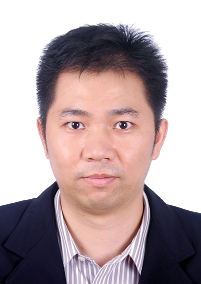 Xuhan Dai (戴旭涵)合作论文数School of Integrated Circuits, Shanghai Jiao Tong University1
 Wei Luo (罗伟)合作论文数School of Materials Science and Engineering, Zhejiang University1




