In this paper, asynchronous receptive circuit of retinal pathway is proposed for cone cells. Cone cells respond differently to different wavelengths of light and they are responsible for color vision. The cells present in retinal pathway namely cone photoreceptor, bipolar cell, amacrine cell and ganglion cell are mimicked using 180 nm Complementary Metal Oxide Semiconductor (CMOS) technology in strong inversion region. The proposed circuit is event based and hence asynchronous in nature. Additionally, amacrine stage is mimicked such that analog multiplexing occurs which is matching with its biological behavior. Both these features give output near to response of actual biological retinal pathway. The circuit detects wavelengths in visible spectrum of light with temporal contrast. At amacrine stage, selectivity is achieved without any external control signal which shows intelligent behavior at analog circuit level. The concept of color sensitivity of cone is considered to generate input stimulus of the circuit using Commission on Illumination (CIE) standard. The power consumed by the entire pathway circuit is 183 mW.
In this paper, we propose a SOI FinFET device based photoreceptor for silicon retina to reduce power consumption. Nowadays, in the field of neuromorphic engineering the main aim of the researcher is to implement a biological nervous system based on silicon devices. Major performance metrics which influence the design of neuromorphic circuits along with biological plausibility are compactness, low power consumption, scalability and computational complexity. Moreover, to process the information biologically billions of neurons consume only a few watts of power. However, present design of silicon photoreceptor consumes power much larger than actual biological photoreceptor. Hence to achieve low power consumption we are using nanometer SOI FinFET device technology. In this paper, output of the outer retinal cell, namely photoreceptors, is reconstructed and verified with the help of developed ionic current based mathematical model of the retina. The model contains non-linear differential equations based on the fundamental framework of the Hodgkin-Huxley model. In order to closely match the biological response, the selection of parameters of membrane voltage and other membrane dependencies through compartments are done using MATLAB simulation. After mathematical verification, the biological behavior of photoreceptor cell of retinal system is mimicked through circuit using 180 nm Metal Oxide Semiconductor Field Effect Transistor (MOSFET) and 32 nm Silicon on Insulator Fin Field Effect Transistor (SOI FinFET) device. It is observed that SOI FinFET based photoreceptor for silicon retina circuit consumes less power in picowatts matching the power consumption of biological retinal system, as compared with MOSFET based circuits.
—In this paper, we proposed a SOI FinFET based ON bipolar cell of silicon retina which plays an important role in neuromorphic applications like differential motion detection. Low power consumption along with biological plausibility is one of the crucial parameters of any neuromorphic retinal circuit as in the brain all biological systems consisting of billions of neurons consume power in terms of a few μwatts. First, the output of linkage cell between inner and outer plexiform layer i.e. bipolar cell is reconstructed and verified using developed ionic current based mathematical model which is established considering Hodgkin-Huxley model as the base model, and then biological behavior of the ON bipolar cell is mimicked through circuit using 180 nm, 90 nm and 45 nm Metal Oxide Semiconductor Field Effect Transistor (MOSFET). The power consumption in each case is obtained to be approximately 18.5 nW, 10.5 nW and 1 nW which is much larger than the power consumed by biological bipolar cell. Moreover, the same circuit is implemented with 32 nm Silicon on Insulator Fin Field Effect Transistor (SOI FinFET) device. It is observed that SOI FinFET based ON bipolar cell consumes 17.5 pW power which is less in comparison to MOSFET based bipolar cell. The output of bipolar cell is matched with biological nature of the waveform in each case.
Neuromorphic circuits are extensively being researched worldwide to emulate biological responses in electronic circuits. Integrated circuits to mimic the behavior of retina are also being modeled and developed. One of the important functions of retina is to identify the moving objects. Starburst amacrine cell is one of the cells in retina which is responsible for detection of differential motion. Researchers have modeled starburst amacrine cell that requires adders as an implicit element. Adders are primarily used for adding responses received from many bipolar cells. This paper is to investigate various types of adders and to identify the adder which would be more suitable for modeling starburst amacrine cell in neuromorphic applications. In this paper, investigation of classical CMOS analog adder, differential analog adder, low power adder, nonlinear adder and op-amp-based adders is carried out. The primary objective is to identify from these adders which would be more suitable in case of differential motion detection and should give near biological response. All the simulations are done using TSMC 180 nm technology.
A bandwidth enhanced multilayer Electromagnetic Band Gap (EBG) structure to reduce the simultaneous switching noise (SSN) in high frequency operating circuits, which useful for the satellite communication application, is presented in this paper. A proposed stack structure is mathematically analyzed by the dispersion method and transmission matrix method. Simulation results show good mitigation of SSN in scattering parameters and signal integrity in terms of eye diagrams. We have also checked for power integrity analysis using self-impedance. The proposed structure gives a good SSN suppression at -30 dB from 817 MHz to 26.32 GHz, around 25.50 GHz bandwidth and also reduces the cavity mode resonance within the stopband range. The proposed multilayer structure is compared with planar EBG plane and reference board. It is also compared with published results.
Simultaneous switching noise (SSN), often occurs when signals transition rapidly between the ground and power planes, is an important problem in high-speed digital circuits. The Electromagnetic Bandgap Structure (EBG) is a novel technique that can help to solve signal integrity and power integrity problems. In this paper, we present a three dimensional coplanar electromagnetic bandgap (EBG) structure to improve Signal Integrity (SI), validated by eye diagram and Power Integrity (PI) shown by self impedance. This proposed planar EBG structure offers effective SSN suppression for frequency ranges between 2.38 GHz and 22.39 GHz, with an average suppression level of -30 dB.
In this paper, an EBG-inspired two element triple band-notched ultra wideband multi input multi output antenna is proposed. The antenna is fabricated with the overall size of 47 $$\times $$ 38 $$\times $$ 0.8 $$\textrm{mm}^3$$ using low cost FR-4 epoxy substrate. Designing and simulation is carried out using Ansys HFSS software. Using single EBG structure, triple band notches at 3.3, 5.72 and 8.32 GHz are obtained satisfying WIMAX, WLAN and uplink satellite X-bands respectively. By inserting inverted L-shaped stubs on the ground plane, an improved isolation better than 25 dB is achieved throughout the UWB range. Surface current distribution and radiation pattern of proposed MIMO antenna in E-plane and H-plane are studied and discussed. Performance parameters such as ECC, DG, CCL, TARC and MEG are also investigated and found to be within the acceptable limits specified for diversity applications. Therefore UWB-MIMO applications wherein triple band-notched MIMO antenna with simplified design, compact size and improved isolation is desired, proposed MIMO antenna will out stand as strong candidature.
Primary motivation of this paper is to design an ADC that is suitable for communication applications with high operating speed in GSPS and fabricate at SCL (Semi-Conductor Laboratory) Chandigarh, India. This paper presents an 8-bit Flash ADC using TIQ (Threshold Inverter Quantization) Comparator and ROM encoder. It has been observed that the DNL is 0.051 *LSB, INL is 1.73*LSB with dynamic power dissipation of 0.277µW, and operating speed of 0.4 GSPS. The application of the implemented ADC in communication has been demonstrated in the SID Antenna receiver. The simulation has been carried out with BSIM 180nm technology in LTspice.
With the population increasing exponentially, there has been a shortage of water in various countries. To help people manage water resources in an appropriate way, a water monitoring and management system needed to be built. Several invasive flow meters are present to cater to the problem but there exist several overhead expenses and issues with it. A good alternative for the above, a non-invasive flow meter, would be a more efficient solution. Though, some non-invasive flow meters exist, they’re expensive and unsuitable for use in some critical scenarios. So, a novel method and system, to calculate the rate of flowing water using audio-processing of the sound of flowing water, was developed. The system would be clamped on the surface of the pipe, unlike other systems which operate from inside the pipe. The flow meter developed using this method would only require a microphone on the sensor’s part, which will make it cost-effective. The process involves an algorithm that processes the sound of water using a microcontroller unit and then computes a single value which then depicts the range of flow rate. Further, using IOT analytics, future predictions and other important metrics would be displayed on a simple yet detailed user interface.
In this paper, a rectangular embedded dual band Electromagnetic Band Gap (EBG) structure at frequencies 2.45/5.8 GHz useful in industrial, scientific, and medical (ISM) band for various wearable applications is proposed. The main intent of this work is to design a dual-band EBG to reduce specific absorption rate (SAR). The unit cell which is a part of the EBG structure is formed using a rectangular patch. It has a U-shaped rectangular slot and a stretched strip with a rectangular patch at end. EBG unit cell simulation is accomplished by solving eigen-mode problem in High Frequency Structure Simulator (HFSS). EBG structure has to be suitably designed and fine tuned for specified band stop property to reduce surface waves. It must improve front to back ratio (FBR). With placing antenna on human body, frequency detuning occurs which is undesirable thus emphasizing the need of improvement in impedance bandwidth. This improvement can be achieved by a suitable design of EBG structure. In this work, the proposed EBG structure is integrated with a dual-band monopole antenna at frequencies 2.45/5.8 GHz for wearable application. The evaluation of antenna performance on a four layer body model is carried out. Simulations are used to demonstrate EBG array structure effectiveness for the reduction of Specific Absorption Rate (SAR) on the four layer body model. Computed SAR values for tissue in 1 g and 10 g are within standard prescribed limits. It is concluded that the proposed dual-band antenna is appropriate for wearable applications. Proposed EBG array is fabricated and integrated with a twin E-shaped monopole antenna. The measurement of reflection coefficient, radiation pattern, and transmission coefficient of fabricated EBG array is carried out. The measured and simulated results show good agreement. Antenna performance in the event of bending condition and on-body condition is assessed.
Self-driving cars being the new technology are gaining attention from all over the globe. This paper deals with the simulation results of an autonomous car trying to learn from its environment which includes static blocks using machine learning. Learning is performed using Deep Q-learning. The neural network computes the Q-values on the basis of the rewards corresponding to the action that the car takes. The autonomous system in the car chooses that particular action that has a maximum reward. The actions are the angles through which the car can steer at a fixed speed. Also, difficulties related to the implementation of autonomous self-driving cars in India have been discussed and possible solutions to them have been presented.
This paper proposes and emphasizes the requirement of an Blockchain based smart contract for NGO's and startup crowdfunding in the present circumstances. It also highlights the need of an online financial system for indigenous NGO's and seed fund utilization of startups. Conventionally, most charity organizations make use of hard cash for settling its transactions making the process less transparent. However, due to the COVID-19 pandemic, financial system has been largely affected. In this case an online financial transaction cum procurement portal would be crucial for the candidates applying relief in remote locations. The system analyses their eligibility based on their Curriculum Vitae (CV). Proposed system uses Ethereum based smart contract and Truffle Box to build a complete Dapp (decentralized application). Authors have used MetaMask Extension as a cryptocurrency wallet and Ganache blockchain to develop, deploy and test the decentralized application.
Design of wearable textile antenna in variety of applications needs novel approaches to achieve objectives of compactness and acceptable Specific Absorption Rate (SAR). Various methods to reduce SAR using various types of EBG structures have been reported in recent past for both single and dual band antenna. Modeling of antenna for dual band 2.4 GHz and 5.8 GHz is carried out for wireless local area network application. In this paper, authors propose compact dual band gap EBG structure. It consists of double concentric ring with slot along with inner patch. Important design performance parameters like reflection phase, reflection coefficient, etc are obtained by simulations. SAR values with this antenna integrated with EBG are computed in HFSS on human arm & male torso model. Simulations results show that proposed EBG array structure is effective for reduction of SAR values to acceptable values.
This paper introduces and validates a compact two-dimensional Electromagnetic Bandgap (EBG) structure for the improvement of signal integrity (SI) and power integrity (PI) by suppressing Simultaneous Switching Noise (SSN). SSN bandwidth can be increased by using the proposed T bridge compact planar structure. The proposed structure is simulated using Ansys HFSS Software. Simulated and measured results by Vector Network Analyzer provide 3.13 GHz to 11.40 GHz frequency bandgap with good mitigation of SSN at -30 dB noise suppression reference. It will almost cover S, C, and X bands from electromagnetic frequency spectrum. This will be useful for satellite and terrestrial communication and radar communication applications. The proposed structure analyzes signal integrity issues using eye diagram in MATLAB and power integrity in HFSS with input impedance respectively. The main purpose of this work is to provide a compact structure to improve signal and power integrity by the suppression of power/ground noise. Comparative study is also performed with the proposed structure and reference board with similar dimensions.
Neuromorphic engineering is multidisciplinary branch of biology, physics, mathematics, neuroscience, electronics engineering and computer science. Neuroscientists are working on mimicking retina, cochlea, motoring neurons etc. For the retinal systems, substantial research has been done due to which understanding of basic components, connection methods and computational processes becomes easier. There are various approaches like mathematical modeling, device modeling, circuit level and system level modeling by which retina can be mimicked. Still researchers get new challenging tasks due to new insights given by neuroscientists into retinal biological system. Due to adaptive nature of human brain, modeling of neurons and synapses is a challenging task. Generally, area, speed and power are the major tradeoffs in any VLSI (Very Large Scale Integration) circuits; however, degree of biological realism and robustness need to be considered in neuromorphic circuits. There are many research papers available in the literature related to modeling of bipolar and ganglion cells, however circuits giving near biological response are the most sought-after circuits. In this paper, spiking behaviour of combined bipolar and ganglion cell is mimicked considering novel averaging and multiplier circuit for bipolar cell, and comparator-based circuit for ganglion cell to mimic the best possible near-biological response. The circuit is implemented using TSMC 180nm technology using LTSpice.
In this manuscript, a CPW fed ultra wide band antenna loaded with electromagnetic band gap superstrate is proposed. EBG structure printed on superstrate is displaced along the length of CPW antenna to achieve multi functional band-notch characteristics. For a particular position of EBG loaded superstrate on CPW antenna substrate, antenna shows single wide band-notched, single narrow band-notched, dual band-notched and UWB characteristics. Simulation of proposed antenna is carried out using Ansys HFSS software. Proposed antenna has bi-directional and omni directional radiation patterns in Electric and magnetic field planes respectively. So, UWB applications demandanding multi functional characteristics within one antenna unit, proposed CPW fed antenna loaded with EBG superstrate proves to be true candidate.
In this paper, a UWB monopole antenna with triple band-notch characteristics using single TBMV-EBG (Triple band multi-via electromagnetic bandgap) unit cell is proposed and demonstrated. The antenna with a fork-type radiating patch with TBMV-EBG is simulated using Ansys HFSS. Measurement results show triple band-notches at 3.39, 5.78, and 8.60 GHz, respectively, which are in good agreement with simulation results. The proposed antenna has bi-directional pattern in E-plane and omnidirectional pattern in H-plane. Moreover, tunable characteristics of the proposed antenna using a single varactor diode are also presented. By changing the capacitance of varactor, the bandnotched antenna is effectively tuned from 2.69–3.46, 5.71–7.84, and 8.40–8.50 GHz. The same antenna structure can be operated at different band notching modes depending upon the varactor’s capacitance. Therefore, the proposed UWB antenna will prove to be a promising candidate wherein multi-band rejections using single TBMV-EBG unit cell and tunability using one varactor diode are desirable.
The severe problem of Gas Geyser Syndrome calls for the need for a gas sensor that can detect the change in concentration of Carbon Monoxide (CO) gas. The existing gas sensors have limitations of low sensitivity and selectivity; accurate detection of CO is important in the case of Gas Geyser. Microfluidic sensors are generally recommended to improve sensitivity and selectivity. This research work proposes the development of a Microfluidic sensor. The principle working is to measure the change in resistance when the gas is exposed to a sensing layer, and micro-heaters are used to provide temperature uniformity to this layer. The geometry of the structure and the environment for sensing the gas was developed using COMSOL Multiphysics® 5.3a. The Meshing of the geometries was done using a combination of both physics-controlled and user-controlled geometry. To test the sensor, a material was specially created which had the properties of CO gas since it is not readily available in software. After filling the chamber with CO gas, the sensor's response was observed by plotting various parameters to ensure the proper working of the sensor in given environmental conditions. For the supply voltage of (1.2V), the uniform temperature profile was observed to be (640K).
The concept of smart cities is emerging and has become popular. The technology is advancing at a fast pace and it has made the concept of smart cities achievable. But as there is increase in number of vehicles and mismanagement of parking spaces, people tend to create congestion whether it be on-street or off-street, which leads to wastage of time and unnecessary pollution. There is an utmost need to develop a smart parking system which would help an individual to find empty parking slot. Although there is ton of research going on for the development of smart parking system but most of them still rely on the old concept of sensor-based approach. In this paper, a prototype of Camera based Smart Parking System is proposed, which detects live empty parking slots and notifies it through a user-friendly Android application.
Radiation environment generates high soft error rates in conventional SRAM. To overcome this issue, several radiation hardened by design SRAM circuits (12TRHBD, 13TRHBD, DICE, etc.) have been developed. Although many of the radiation hardened SRAM cells are there, all the circuits mainly concern a single node upset only. In this chapter, 16T radiation hardened static random-access memory bit cell is designed and verified for a single node and multi-node upset. RHBD 16T bit cell is designed with SAED-PDK 32nm technology and compared with recently reported RHBD 12T and has a 99% improvement in recovery rate. Simulation results show that RHBD 16T is more resilient to a single node and multi-node upset. This shows that the proposed RHBD16T cell is highly tolerant against radiation strikes.
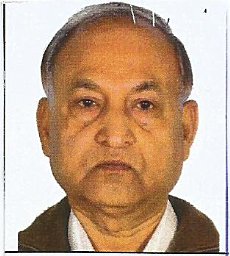 Ashok K Saxena合作论文数16
 Sudeb Dasgupta合作论文数Semiconductor Devices and VLSI Technology Group, Indian Institute of Technology15
 Shah, Payal合作论文数13
 Pramod P. Bhavarthe合作论文数Dept Artificial Intelligence & Data Sci, Vasantdada Patil Pratishthans Coll Engn & Visual A9
 Reena Sonkusare合作论文数9Manisha Bansode合作论文数7
 Prashant Kasambe合作论文数Sardar Patel Institute of Technology6
 Vijay Ramesh Kapure合作论文数S.P.I.T5
 Vidya R. Keshwani合作论文数4
 K. T. V. Reddy合作论文数Datta Meghe Institute of Medical Sciences4Sushma Srivastava合作论文数3
 Gaurav Kaushal合作论文数VLSI Design Laboratory ABV-Indian Institute of Information Technology, Management at Gwalior3
 Dhananjay R. Kalbande合作论文数Department of Computer Engineering, Sardar Patel Institute of Technology, Mumbai, India2
 Narendra Bhagat合作论文数Electronics Dept., Sardar Patel Institute of Technology2Poladia, Meet合作论文数2
 Soura Dasgupta合作论文数Department of Electrical and Computer Engineering, University of Iowa;Department of Applied Mathematical and Computational Sciences, University of Iowa;College of Engineering, University of Iowa;Iowa Technology Institute, University of Iowa2Ajay Prajapati合作论文数2D. V. Bhoir合作论文数1Pradhuman Singh合作论文数1Nitish Wadhavkar合作论文数1Aditya Tarade合作论文数1Vinay Vishnani合作论文数1Shraddha Mayekar合作论文数1Nachiket Nanadikar合作论文数1Kapil Majumder合作论文数1Jinalkumar Doshi合作论文数1
 Soham Pinge合作论文数1Ninad Chitnis合作论文数1Vikramaditya Dangi合作论文数1Lance Fernandes合作论文数1Zalak Dave合作论文数1
 Snehal Lopes合作论文数Electronics and Telcommunication Department, St. Francis Institute of Technology1
 Shridhar R. Sahu合作论文数University of Mumbai1Kumar Khandagle合作论文数1Pratik Pai合作论文数Sardar Patel Institute Of Technology1
 Harsh Agarwal合作论文数Sardar Patel Institute of Technology1
 CH Naga Raghuram合作论文数1
 akshata raut合作论文数1pawankumar fakatkar合作论文数1sachin hatture合作论文数1
 Ganesh Gore合作论文数University of Utah, Electrical and Computer Engineering Department, Salt Lake City, Utah, USA1Saurabh Acharya合作论文数Dept Elect Engn & Comp Sci, Univ Michigan1
 Manhas, S.K.合作论文数1Langalia, H.合作论文数1Gharpure, P.合作论文数1Kabra, H.合作论文数1Agrawal, K.R.合作论文数1
 Manisha Pattanaik合作论文数Department of Information Technology, Indian Institute of Information Technology and Management1
 Satish Maheshwaram合作论文数1




