The influence of electron irradiation on the resistance of the NOVER-1 resist to ion-beam etching is studied. Etching is carried out by argon ions with energies between 300 and 2500 eV. It is found that, depending on the energy and angle of incidence of the ions on the surface of the resist, electron irradiation may either speed up or slow down the NOVER-1 etching. A clear correlation is observed between the penetration depth of the ions in the resist and the influence of the electron irradiation on the resistance of the resist to etching. At ion energies higher than 500 eV (ion penetration depth ≳3.5 nm) the resistance decreases, passes through a minimum at low electron irradiation doses, and returns to the etching rate of the initial resist at high doses. For glancing etching angles (∼ 70° to the surface normal) and low ion energies (300 eV), i.e., small ion penetration depths (≲2.5 nm), an electron-irradiated resist is etched more slowly than the initial resist at all the electron irradiation doses studied. This effect may be used to enhance the resistance of resist structures whose height exceeds their width, which in this case is determined mostly by the rate of etching of the inclined facets.
The structure of the photon states and dispersion of cavity polaritons in semiconductor microcavities with two-dimensional optical confinement (photon wires), fabricated from planar Bragg structures with a quantum well in the active layer, are investigated by measuring the angular dependence of the photoluminescence spectra. The size quantization of light due to the wavelength-commensurate lateral dimension of the cavity causes additional photon modes to appear. The dispersion of polaritons in photon wires is found to agree qualitatively with the prediction for wires having an ideal quantum well, for which the spectrum is formed by pairwise interaction between exciton and photon modes of like spatial symmetry. The weak influence of the exciton symmetry-breaking random potential in the quantum well indicates a mechanism of polariton production through light-induced collective exciton states. This phenomenon is possible because the light wavelength is large in comparison with the exciton radius and the dephasing time of the collective exciton state is long.
Copper films were deposited onto oxidized silicon wafers by the self-ion assisted technique. A 0 and 6 kV bias was applied to the substrate during the deposition. The films were patterned into parallel line arrays of 20 lines 0.5 mm long, using electron lithography and dry etching. After patterning, the lines were covered by silicon oxide and annealed in vacuum for 1 hour at the temperature 450 degrees C. Electromigration testing was performed in air in the temperature range from 280 degrees to 350 degrees C and at a current density 3.10(6) A/cm(2).It was found that the resistivities of the films deposited at 6 kV and without bias were 1.7 and 2.0 mu Omega . cm, respectively. The median times to failure are 398.6 and 240 h and the deviations in the time to failure are 0.8 and 0.54 for 6 kV lines and 0 kV lines, respectively. An electromigration activation energy of 0.89 eV was found for 0 kV films.
 Vn Matveev合作论文数1
 V. T. Volkov合作论文数1m fraenkel合作论文数1TA Pikuz合作论文数1
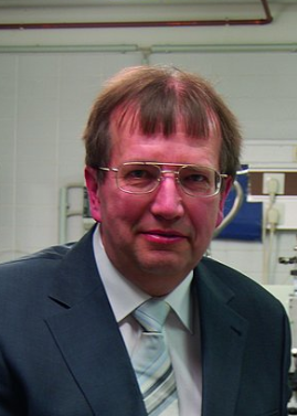 Alfred Forchel合作论文数Technische Physik, Universitat Wurzburg1T.B. Borzenko合作论文数1
 Alexander Tartakovskii合作论文数School of Mathematical and Physical Sciences, University of Sheffield;Near-Field Optical Imaging and Spectroscopy Centre, University of Sheffield1
 V. T. Petrashov合作论文数1
 Oleg V. Kononenko合作论文数Russian Academy of Sciences Institute of Microelectronics Technology and High Purity Materials Chernogolovka1L. A. Panchenko合作论文数1S. V. Dubonos合作论文数1D. V. Kulakovskii合作论文数1
 Arie Zigler合作论文数The Racah Institute of Physics, Faculty of Science, The Hebrew University of Jerusalem;Department of Physics, The Hebrew University of Jerusalem1
 Johann Peter Reithmaier合作论文数Institute of Physics, The Faculty of Mathematics and Natural Sciences, University of Kassel;Institute of Nanostructure Technologies and Analytics, University of Kassel1
 Anatoly Firsov合作论文数1Anatoly Faenov合作论文数1




