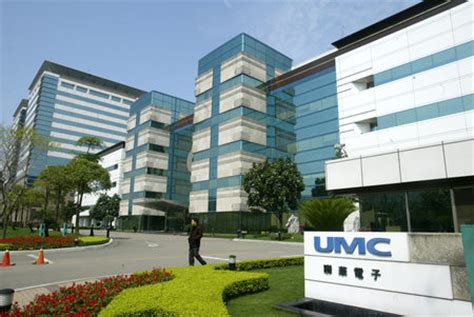
联电(联华电子股份有限公司)是半导体晶圆制造业的领导者,提供先进制程技术与晶圆制造服务,为IC产业各项主要应用产品生产芯片。
The 3-D integrated circuit (3DIC) technologies have attracted attention due to the advantages of smaller size, higher speed digital performance, and low-power consumption in integrated circuits. Hybrid bonding is a key technology for advanced 3-D packaging that offers shorter signal transmission paths through bumpless connections. While most studies on the influence of different annealing conditions on bonding quality have focused on postannealing evaluations, there is significant potential for further exploration into in situ analyses. This study introduces a novel approach, an in situ electrical measurement, for the real-time monitoring of hybrid bonding processes. It aims to reduce manufacturing costs and enhance product quality by investigating critical heating conditions. Furthermore, the effects of temperature and ramping rate on bonding behavior are investigated. This study demonstrates the feasibility of achieving hybrid bonding at 235 degrees C with a brief dwell time of 1.5 min, under these experimental design and fabrication processes.
A novel FinFET device structure is proposed to achieve a balanced design between Electrostatic Discharge (ESD) robustness and Electrical Overstress (EOS) Surge immunity for FinFET integrated circuits (ICs). FinFET devices become increasingly susceptible to long pulse EOS events due to reduced effective silicon volume, worse thermal dissipation, and lower breakdown voltage. Currently, industry practices primarily depend on circuit design methodologies to mitigate EOS Surge events. However, several critical challenges must be addressed in circuit design, including design complexity, response delay, and power consumption. To overcome these issues, a component-level solution on the FinFET device with merged LDD implantation under the dummy gate was proposed to effectively enhance HBM robustness and Surge immunity of the power-rail clamp circuit. Notably, these improvements were achieved without the necessity for additional mask or process step, simplifying the fabrication process, and reducing both manufacturing costs and complexity for using in FinFET ICs.
Technological advancements continue to change the nature of job content and task requirements. As a result, employees may feel that their knowledge, skills, and abilities no longer match the current job requirements (i.e., low demands-abilities fit), which can negatively impact their performance outcomes. Drawing on the perspectives of incentive and sorting effects, we propose that perceived performance-reward contingency will mitigate the detrimental effects of low D-A fit on work-avoidance behaviors and task performance. Additionally, we hypothesize that the moderating effect of perceived performance-reward contingency will be particularly pronounced for employees with high job sacrifice. Utilizing a multisource and multiphase research design, we collected data from 332 supervisor-employee pairs across diverse industries in Study 1, and from 218 supervisor-employee pairs in the high-technology industry in Study 2. In both studies, we found consistent support for our hypotheses. Specifically, the results indicate that when perceived performance-reward contingency is high, the detrimental effects of low D-A fit on work-avoidance behaviors and task performance are less pronounced. Our findings also support the hypothesis that job sacrifice amplifies the moderating effect of perceived performance-reward contingency. Our study contributes to literature by providing insights into how to effectively manage employees experiencing low D-A fit.
This work presents a systematic investigation of the impact of gate-to-sinker Lgsink scaling on threshold voltage Vth stability of n-type lateral double-diffused MOS (n-LDMOS). The effects of Lgsink were examined experimentally. A unique dependence of threshold voltage on gate-to-sinker spacing was identified, originating from boron diffusion of the P++ sinker into the channel and drain LDD regions during high-temperature drive-in. This mechanism was validated by secondary ion mass spectrometry (SIMS) profiling, which directly demonstrated boron penetration beneath the channel. The increased channel doping accounts for the observed rise in threshold voltage and reduction in drive current. These findings highlight the necessity of co-optimizing geometric scaling and diffusion control to achieve better control of Vth in advanced lateral double-diffused metal-oxide-semiconductor (LDMOS) technologies.
Most defect classification methods rely on deep learning, which requires human effort for image annotation. However, acquiring large, high-quality labeled datasets is often impractical due to time and cost constraints. In this paper, we propose an approach, which leverages a pretrained vision-language model with automatic prompt engineering, to reduce dataset dependence. By optimizing prompts, our approach enables accurate classification, even for unknown pad defects. Experimental results demonstrate that our approach achieves higher accuracy compared to CNN-based models and VLM-based methods on a dataset from a semiconductor company.




