Silicon p-type samples irradiated with 6 MeV and 4 MeV electrons (fluence range from 0.4 to 5x1016cm-2) were analyzed simultaneously using Hall and magnetoresistivity (MR) effects to evaluate the accumulated damage to the material. The measurements, performed in the 100-400 K temperature range, showed a significant drop in the Hall signal at lower temperatures, while the MR remained high. The charge carrier density dependence on temperature revealed thermal activation energies, which were attributed to known point defects. By combining these results with the carrier mobility data, the variation in total defect density with irradiation fluence was evaluated. Additionally, the annealing of the irradiated materials was performed, and the observed changes were recorded.
A consistent quantitative description of radiation-induced degradation on p-type Silicon detectors is conducted within CERN RD50 collaboration. The present contribution summarizes the first obtained results for epitaxial 50 µm thin pad diodes irradiated with protons, neutrons and gamma rays. Microscopic and Macroscopic damage-driven effects are analyzed.
Minority carrier traps play an important role in the performance and radiation hardness of the radiation detectors operating in a harsh environment of particle accelerators, such as the up-graded sensors of the high-luminosity hadron collider (HL-HC) at CERN. It is anticipated that the sensors of the upgraded strip tracker will be based on the p-type silicon doped with boron. In this work, minority carrier traps in p-type silicon (Si) and silicon–germanium (Si1−xGex) alloys induced by 5.5 MeV electron irradiation were investigated by combining various modes of deep-level transient spectroscopy (DLTS) and pulsed technique of barrier evaluation using linearly increasing voltage (BELIV). These investigations were addressed to reveal the dominant radiation defects, the dopant activity transforms under local strain, as well as reactions with interstitial impurities and mechanisms of acceptor removal in p-type silicon (Si) and silicon–germanium (SiGe) alloys, in order to ground technological ways for radiation hardening of the advanced particle detectors. The prevailing defects of interstitial boron–oxygen (BiOi) and the vacancy–oxygen (VO) complexes, as well as the vacancy clusters, were identified using the values of activation energy reported in the literature. The activation energy shift of the radiation-induced traps with content of Ge was clarified in all the examined types of Si1−xGex (with x= 0–0.05) materials.
The value of exchange energy for near-surface double-donor and double-quantum dot structures under the effect of external electric field has been calculated using unrestricted Hartree–Fock method. The dependences of exchange energy on geometric parameters have been obtained. It has been found that the location of donor centers near the surface of the semiconductor leads to an increase in the exchange energy. Approximate formulas for the dependence of the exchange energy on the distance between the centers of quantum dots are suggested. It has been shown that exchange coupling control is less sensitive to electric field as compared to magnetic field, and electron density relocation at large electric fields should be taken into account when designing devices based on the structures under study.
The particle detector degradation mainly appears through decrease of carrier recombination lifetime and manifestation of carrier trapping effects related to introduction of carrier capture and emission centers. In this work, the carrier trap spectroscopy in Si1−xGex structures, containing either 1 or 5% of Ge, has been performed by combining the microwave probed photoconductivity, pulsed barrier capacitance transients and spectra of steady-state photo-ionization. These characteristics were examined in pristine, 5.5 MeV electron and 1.6 MeV proton irradiated Si and SiGe diodes with n+p structure.
In this work, electrically active defects of pristine and 5.5 MeV electron irradiated p-type silicon–germanium (Si1−xGex)-based diodes were examined by combining regular capacitance deep-level transient spectroscopy (C-DLTS) and Laplace DLTS (L-DLTS) techniques. The p-type SiGe alloys with slightly different Ge contents were examined. It was deduced from C-DLTS and L-DLTS spectra that the carbon/oxygen-associated complexes prevailed in the pristine Si0.949Ge0.051 alloys. Irradiation with 5.5 MeV electrons led to a considerable change in the DLT spectrum containing up to seven spectral peaks due to the introduction of radiation defects. These defects were identified using activation energy values reported in the literature. The double interstitial and oxygen complexes and the vacancy, di-vacancy and tri-vacancy ascribed traps were revealed in the irradiated samples. The interstitial carbon and the metastable as well as stable forms of carbon–oxygen (CiOi* and CiOi) complexes were also identified for the electron-irradiated SiGe alloys. It was found that the unstable form of the carbon–oxygen complex became a stable complex in the irradiated and the subsequently annealed (at 125 °C) SiGe samples. The activation energy shifts in the radiation-induced deep traps to lower values were defined when increasing Ge content in the SiGe alloy.
In view of the HL-LHC upgrade, radiation-tolerant silicon sensors containing low-resistivity p-type implants or substrates, like LGAD or HV-CMOS devices, are being developed in the framework of ATLAS, CMS, RD50 and other sensor R&D projects. These devices are facing a particular problem — the apparent deactivation of the doping due to the irradiation, the so-called acceptor removal effect. In the present work proton and neutron fluence-dependent radiation damage effects, including the change in leakage current and effective doping concentration, space charge sign-inversion, but also introduction and annealing of point- and cluster-like defects have been studied in Si pad diodes fabricated from p-type EPI material of different resistivity (10–1000 Ωcm). Standard electrical characterisations (IV, CV), TCT (Transient Current Technique) and TSC (Thermally Stimulated Current) techniques were applied. A correlation between effective doping concentration obtained from CV measurements and defect concentration Nt extracted from TSC measurements for both – neutron and proton – irradiations was observed pointing towards the microscopic origin of the acceptor removal. A detailed analysis of the dominant TSC peaks - E(30), BiOi and three main deep acceptor levels H(116), H(140) and H(152) - responsible for the changes in the effective space charge is performed. The origin and annealing behaviour of E(30) and H(40) and other cluster-related defects are discussed as well.
Numerical methods to calculate electronic states of isolated donor coupled to electrically defined quantum dot are developed. The donor-dot system is described with the use for stationary Schrodinger and Laplace (Poisson) equations. Energy spectra of an electron bound to the donor and quantum dot are calculated using the finite difference and finite element methods. It is shown that when developing the finite difference method, the singularity at the donor location should be taken into account using cusp condition. Asymptotic boundary conditions to calculate confining electric fields are proposed. Main sources of errors related to numerical calculations are analyzed. Dependences of critical parameters on the size of a disc-shaped controlling gate and external magnetic field are determined for donor qubit.
The influence of the injection of minority charge carriers on the formation of a divalent bistable defect (DBH) having two energy levels of Ev + 0.44 eV and Ev + 0.53 eV in its metastable configuration is investigated. Using forward current injection, the formation temperature of this defect in p‐type silicon can be lowered by about 50 °C. The production of such bistable defect is enhanced in materials with a high ratio of boron to carbon concentrations. This allows one to conclude that the boron atom is one of the constituents of the defect under study. There is also a correlation between the behavior of the bistable hole traps and a metastable electron trap observed earlier. It is concluded that these traps are related to metastable and stable configurations of the DBH defect, which has inverse occupancy level ordering in its stable configuration.
Comparative studies employing Deep Level Transient Spectroscopy and C-V measurements have been performed on recombination-enhanced reactions between defects of interstitial type in boron doped silicon diodes irradiated with alpha-particles. It has been shown that self-interstitial related defects which are immobile even at room temperatures can be activated by very low forward currents at liquid nitrogen temperatures. Their activation is accompanied by the appearance of interstitial carbon atoms. It has been found that at rather high forward current densities which enhance BiOi complex disappearance, a retardation of Ci annealing takes place. Contrary to conventional thermal annealing of the interstitial boron-interstitial oxygen complex, the use of forward current injection helps to recover an essential part of charge carriers removed due to irradiation.
Numerical modeling of electronic state evolution due to non-uniform external electric field in the structure metal-insulator-semiconductor with solitary donor center is carried out. Considering a nanometer disc-shaped gate as a source of the electric field, the problem for the Laplace equation in multilayered medium is solved numerically to determine the distribution of the gate potential. The energy spectrum of a bound electron is calculated from the problem for the stationary Schrödinger equation. Finite difference schemes are constructed to solve both the problems. Difference scheme for the Schrödinger equation takes into account cusp condition for the wave function at the donor location. To solve the problem for the Laplace equation, asymptotic boundary conditions for approximating the external field potential at large distances from the gate in different layers are suggested. These conditions allow to reduce the calculation domain for the electrostatic problem essentially. The effect of the boundary conditions on the accuracy of calculating the potential and energies is investigated. Using the developed difference schemes, the dependences of the energy spectrum of the bound electron on the gate potential are calculated, and the values of critical potential at which the wave function of the electron is relocated are determined. It has been found on the basis of calculation results, that governing parameter for the description of electronic behavior is the potential difference between the donor and semiconductor surface. It has been shown that critical potential difference does not depend on dielectric thickness and permittivity.
With the use of deep level transient spectroscopy (DLTS) the effect of injection of minority charge carriers (electrons) on an annealing rate of self di-interstitial – oxygen (I2O) complex in silicon has been studied. The complex has been formed by irradiation of epitaxial boron-doped n+–p diode structures with alpha-particles at room temperature. It has been shown that the disappearance of this complex at room temperature begins at a direct current density of ~1.5 A/cm2. This characteristic current density has been found for 10 W·cm p-type silicon when the total radiation defect density was less than 15 % of the initial boron concentration, a divalent hole trap with energy levels of Ev + 0.43 eV and Ev + 0.54 eV has been found to appear as a result of recombination-enhanced annealing of the I2O. When the I2O complex is annealed thermally, the concurrent appearance of an electron trap with an energy level of Ec – 0.35 eV has been observed. It has been shown that the divalent hole trap represents a metastable configuration (BH-configuration) of the bistable defect, whereas the electron trap is stab le in the p-Si configuration (ME-configuration). From the comparison of DLTS signals related to different defect configurations it is found that the ME-configuration of this bistable defect can be characterized as a center with negative correlation energy. It has been shown that the injection-stimulated processes make it very difficult to obtain reliable data on the formation kinetics of the bistable defect in the BH-configuration when studying the thermal annealing of the I2O complex.
This work focuses on the kinetic mechanisms responsible for the annealing behavior of radiation cluster-related defects with impact on the electrical performance of silicon sensors. Such sensors were manufactured on high resistivity n-type standard float-zone (STFZ) and oxygen enriched float-zone (DOFZ) material and had been irradiated with mono-energetic electrons of 3.5 MeV energy and fluences of 3 × 1014 cm−2 and 6 × 1014 cm−2. After irradiation, the samples were subjected either to isochronal or isothermal heat treatments in the temperature range from 80 °C to 300 °C. The specific investigated defects are a group of three deep acceptors [H(116 K), H(140 K), and H(152 K)] with energy levels in the lower half of the band gap and a shallow donor E(30 K) with a level at 0.1 eV below the conduction band. The stability and kinetics of these defects at high temperatures are discussed on the basis of the extracted activation energies and frequency factors. The annealing of the H defects takes place similarly in both types of materials, suggesting a migration rather than a dissociation mechanism. On the contrary, the E(30 K) defect shows a very different annealing behavior, being stable in STFZ even at 300 °C, but annealing-out quickly in DOFZ material at temperatures higher than 200 °C , with a high frequency factor of the order of 1013 s−1. Such a behavior rules out a dissociation process, and the different annealing behavior is suggested to be related to a bistable behavior of the defect.
Numerical modeling of electronic state evolution due to external electric field in the structure metal-insulator-semiconductor with solitary donor center is carried out. Considering a nanometer disc-shaped gate as a source of the electric field, the problem for the Laplace equation in infinite multilayered medium is solved to determine the gate potential. The energy spectrum of a bound electron is calculated from the problem for the stationary Schrodinger equation. Finite difference schemes are constructed to solve both the problems. Difference scheme for the Schrodinger equation takes into account cusp condition for the wave function at the donor location. To solve the problem for the Laplace equation, asymptotic boundary conditions for approximating the potential at large distances from the gate are proposed. On the basis of calculation results, a controlling parameter is suggested, which allows to determine the localization of electron wave function regardless of insulator thickness and permittivity.
The electrical characteristics of epitaxial layers of n-4H-SiC (CVD) irradiated with 0.9 and 3.5MeV electrons are studied. It is shown that the donor removal rate becomes nearly four times higher as the energy of impinging electrons increases by a factor of 4, although the formation cross section of primary radiation defects (Frenkel pairs in the carbon sublattice) responsible for conductivity compensation of the material is almost energy independent in this range. It is assumed that the reason for the observed differences is the influence exerted by primary knocked-out atoms. First, cascade processes start to manifest themselves with increasing energy of primary knocked-out atoms. Second, the average distance between genetically related Frenkel pairs grows, and, as a consequence, the fraction of defects that do not recombine under irradiation becomes larger. The recombination radius of Frenkel pairs in the carbon sublattice is estimated and the possible charge state of the recombining components is assessed.
Проведено исследование электрофизических характеристик эпитаксиальных слоев n-4H-SiC (CVD) при его облучении электронами с энергиями 0.9 и 3.5 МэВ. Показано, что скорость удаления доноров увеличивается почти в 4 раза с ростом энергии бомбардирующих электронов в 4 раза, хотя сечение образования первичных радиационных дефектов (пар Френкеля в подрешетке углерода), ответственных за компенсацию проводимости материала, в этом диапазоне практически не зависит от энергии. Предположено, что причиной наблюдаемых различий является влияние первично выбитых атомов. Во-первых, с ростом энергии первично выбитых атомов начинают сказываться каскадные процессы. Во-вторых, увеличивается среднее расстояние между генетически родственными парами Френкеля и как следствие увеличивается доля не рекомбинирующих при облучении дефектов. Проведены оценки радиуса рекомбинации пары Френкеля в подрешетке углерода и возможного зарядового состояния рекомбинирующих компонент. DOI: 10.21883/FTP.2017.03.44199.8399
The effect of an external electric field on the states of a shallow donor near a semiconductor surface is numerically simulated. A disk-shaped metal gate is considered as an electric-field source. The wavefunctions and energies of bound states are determined by the finite-element method. The critical characteristics of electron relocation between the donor and gate are determined for various gate diameters and boundary conditions, taking into account dielectric mismatch. The empirical dependences of these characteristics on the geometrical parameters and semiconductor properties are obtained. A simple trial function is proposed, which can be used to calculate the critical parameters using the Ritz variational method.
Processes of radiation defect formation and cond uctivity compensation in identical silicon carbide samples irradiated with 0.9 and 3.5 MeV electrons w ere compared for the first time. n-SiC (4H) epitaxial layers with thickness of 50 μm were grown in a commercial horizontal hotwall CVD-system at the Leibniz Institute for Crysta l Growth, Berlin, Germany. Commercial SiC (4H) wafers served used as substrates. The electron concentration due to uncompensated donors, n = ND−NA, did not exceed 2 ⋅10 cm in these layers. Schottky diode structures w re fabricated on the SiC layers. The sample irradiation and measurement procedures used in the present study were described in detail in [1]. Figure 1 shows experimental values of the carri er emoval rate in silicon carbide ( ηe), obtained in the present study for two electron energies, 0.9 an d 3.5 MeV, and in [2, 3] for the energy range (6-8) MeV. It can be seen in Fig. 1 that the values of ηe for the case of irradiation with 8 MeV electrons are approximately an order of magnitude larger than t ose for 0.9 MeV electrons. The same figure shows how the calculated Frenkel pair formation rat e ηFP for silicon carbide depends on the energy of bombarding electrons. It can be seen that the ca lculated rate of Frenkel pair formation under irradiation with 0.9 MeV electrons is only twice th a for 0.9 MeV electrons. Thus, it is rather difficult to attribute the experimental data to a s imple increase in the generation rate of radiation defects due to the interaction with impinging parti cles and primary knock-on atoms (PKAs).
 Leonid I. Murin合作论文数17
 Michael Moll合作论文数16E. A. Levchuk合作论文数12I. Pintilie合作论文数11F.P. Korshunov合作论文数11S. B. Lastovskii合作论文数10Eckhart Fretwurst合作论文数9S. B. Lastovski合作论文数8Eugenijus Gaubas合作论文数8
 V. P. Markevich合作论文数7
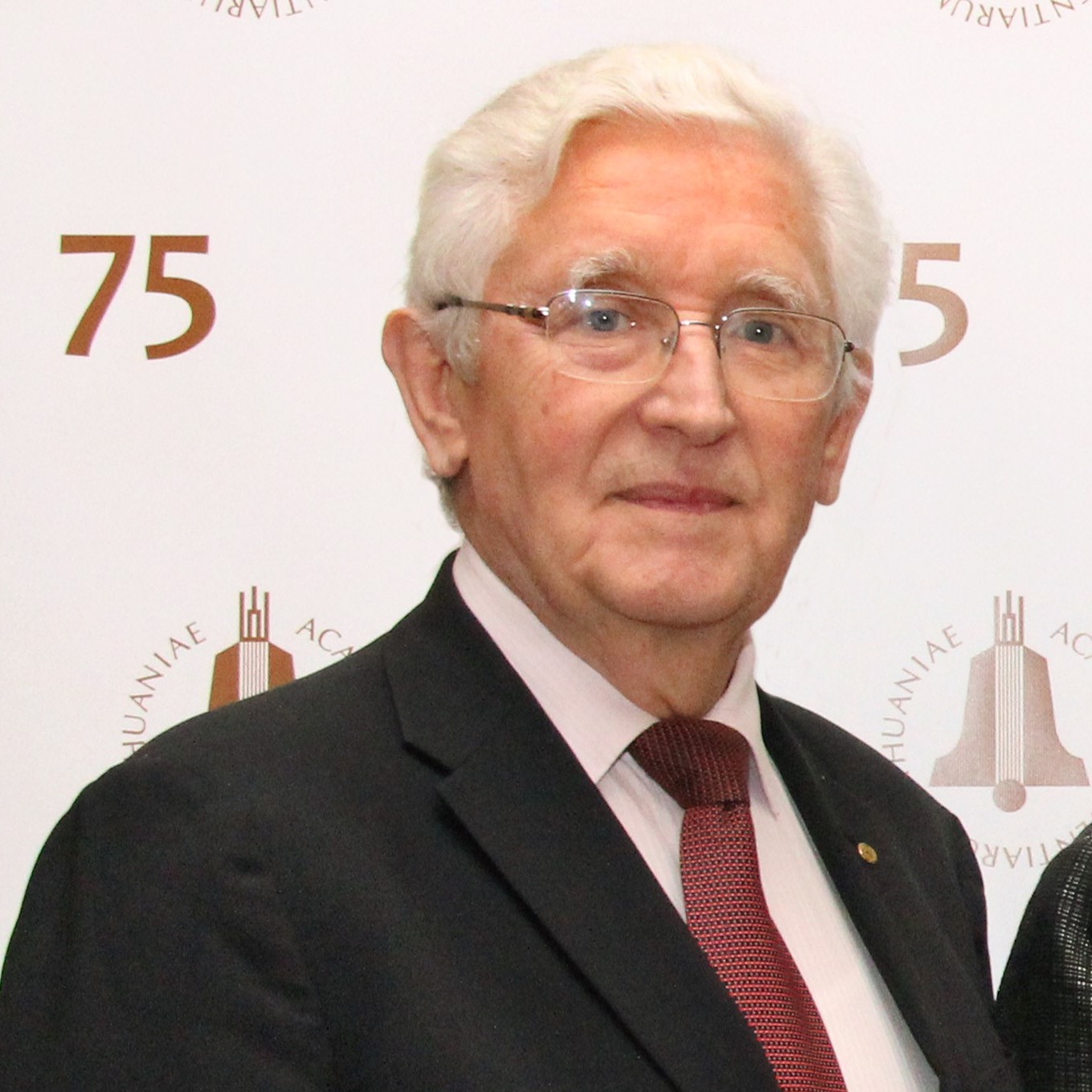 Juozas Vidmantis Vaitkus合作论文数Institute of Photonics and Nanotechnology, Faculty of Physics, Vilnius University5
 J. Storasta合作论文数5
 N. Kazuchits合作论文数Belarusian State University5Vytautas Rumbauskas合作论文数4If Kononyuk合作论文数4Pavlov Jevgenij合作论文数4Gunnar Lindstrom合作论文数4V. A. Gurinovich合作论文数4
 Ioana Pintilie合作论文数Institute of Physics and Technology of Materials4Algirdas Mekys合作论文数4H. S. Yakushevich合作论文数3Kornelijus Pukas合作论文数3Vd Tkachev合作论文数3
 Olga Lavrova合作论文数university of new mexico3Tomas Ceponis合作论文数3
 Vitalii V. Kozlovski合作论文数St. Petersburg State Polytechnical University3Ya. I. Latushko合作论文数3GU Pignatel合作论文数2P. Kodys合作论文数2D. Creanza合作论文数2sergio gonzalez sevilla合作论文数2Наталья Михаиловна Лапчук合作论文数2j nysten合作论文数2A. Zaluzhny合作论文数2v i khivrich合作论文数2R. Radu合作论文数2G. Sellberg合作论文数2D. Stolze合作论文数2A. Litovchenko合作论文数2N. I. Zamiatin合作论文数2L. A. Polivtsev合作论文数2S. Kwan合作论文数2J. Guskov合作论文数2S. Marunko合作论文数2E. Forton合作论文数2D. Naoumov合作论文数2H. Uebersee合作论文数2
 Václav Vrba合作论文数Faculty of Nuclear Sciences and Physical Engineering, Czech Technical University in Prague2S. Assouak合作论文数2




