Compute-in-Memory (CIM) offers an efficient approach for accelerating DNNs by performing matrix–vector multiplications directly within memory. However, its adoption in edge devices is limited by unstable power supplies and the performance overhead of conventional row- or column-wise computing. This paper presents a two-directional CIM-based nvSRAM cell that performs both row- and column-wise operations, enabling faster and more efficient matrix–vector multiplication. The proposed design stores the CIM outputs within the same computation cycle, referred to as Simultaneous Compute and Write (SCW), thereby reducing latency during complex neural network inference. By integrating a single I-MTJ into each SRAM cell, it also provides reliable data retention and restoration during power failures, making it well-suited for low-power, energy-constrained edge applications. Post-layout simulations were conducted to evaluate the proposed architecture. The detailed post-layout simulation results demonstrate a 31% improvement in write margin, a 40% reduction in PDP in memory mode, and an 85% reduction in energy in backup scenarios, compared to state-of-the-art designs. Furthermore, the proposed design achieves a 39.2% EDP reduction during neural network inference operation under power instability, highlighting its suitability for low-power edge computing.
Purpose Prior 12T hybrid SRAM cells offer high stability but introduce practical limitations like high control overhead and complex layouts, hindering large-array integration. This paper aims to propose a novel 12T topology overcoming these VLSI challenges while delivering exceptionally fast read operations.Design/methodology/approach A novel 12T hybrid tunnel field-effect transistor (TFET)-fin field-effect transistor (FinFET) SRAM is proposed. Unlike prior work focused on N-TFET pull-down paths, it introduces an innovative stacked four-PTFET pull-up network. The cell is validated using 20 nm InAs TFET and predictive technology model for multi-gate FinFET in simulation.Findings The architecture eliminates column-based write-assist signals, significantly reduced control complexity, while stacked PTFETs enable area-efficient device overlapping. Leveraging FinFETs in a decoupled read path, the cell achieves an exceptional 24 ps read latency at 0.6 V - outperforming 8T_S and HF_10T cells by approximately 130 & times; and approximately 20 & times;, respectively. Additionally, it secures the highest HSNM and RSNM among evaluated topologies (11% RSNM gain over recent 12T designs) and reduces leakage power by three orders of magnitude compared to the reference O_7T cell by effectively eliminating TFET reverse-bias currents.Originality/value This work presents the first hybrid 12T topology that resolves critical control-overhead and layout limitations while simultaneously shattering the read-speed bottleneck of TFET-based memories.
Abstract The rapid advancement of semiconductor technologies and the increasing demand for high-speed, low-power systems have posed severe challenges, such as increased leakage current and cell instability, in static random access memory. Technology scaling to the nanometer regime exacerbates these issues, necessitating novel circuit solutions. Integrating carbon nanotube field-effect transistors (CNTFETs) with ternary static random access memory (TSRAM) architecture presents a promising approach to enhance data density and energy efficiency. This paper proposes a robust CNTFET-based TSRAM cell design utilizing a controllable inverter-based access mechanism, denoted as the NOTIF1 gate, within the write path. In the proposed architecture, leakage paths are mitigated and conventional storage node conflicts are eliminated through the isolation of the write path and the restructuring of the hold module. Simulations were conducted using the standard Stanford CNTFET model at the 32 nm technology node within the HSPICE environment. The results demonstrate the superiority of the proposed design, which exhibits a hold static noise margin of 194 mV—representing at least a 10% improvement over state-of-the-art counterparts. Furthermore, it achieves an impressive reduction of up to 45% in the write power-delay product. Finally, Monte Carlo simulations verify the robustness of the proposed cell against process variations, confirming its reliability for high-density integration. These attributes render the proposed cell a highly suitable candidate for internet of things applications and energy-efficient systems.
This work presents two innovative 12T cells combining tunnel field-effect transistor (TFET) and fin field-effect transistor (FinFET) technologies. These cells address reverse bias current issues by incorporating separate paths for reading data and write enhancement cut transistors, enhancing hold/read/write static noise margin (H/ R/WSNM), reducing read time, and minimizing power consumption from TFET leakage. At 0.6 V, the first (second) SRAM cell shows a WSNM improvement over O_7T, 8T, CA_10T, 12T, and HF_10T cells by 152 % (93 %), 152 % (93 %), 157.7 % (97.5 %), 95 % (50 %), and 104 % (57 %), respectively. The leakage power of the first (second) 12T TFET SRAM cell is two (four) orders of magnitude lower than O_7T and 8T SRAM cells. These hybrid SRAM cells also exhibit faster read operations across VDD voltage levels (0.3 V-1 V) and the first 12T cell demonstrates shorter write access times than 12T and CA_10T SRAM cells. These characteristics make the proposed cells particularly suitable for energy-efficient IoT devices and medical applications, where balancing power, area, performance, and data integrity is critical.
Approximate computing is one of the promising techniques in error-resilient applications to overcome high-density integration challenges, such as energy consumption and performance. Multipliers constitute a significant portion of computer arithmetic units, leading to considerable energy and time consumption. In this paper, we propose low-power and compact approximate compressors for composing approximate Dadda multiplier structures, including compressors, half adders, and full adders, which utilize three-phase partial product compression: truncated, approximation, and exact columns. In approximate columns, we consider approximate compressors derived from the truth table of the exact 4:2 compressor and simplified K-map entries based on the probability of each combination of inputs. An error-correcting module (ECM) is designed to distinguish specific cases and reduce the error metrics. All circuits were simulated using ModelSim and then synthesized using Design Compiler with the 15 nm FinFET technology. When compared to state-of-the-art works, our multipliers exhibit approximately 30%, 43%, and 10% reductions in power, area, and delay, respectively. To evaluate their functionality, we conducted image multiplication and implemented a simple multi-layer perceptron (MLP) neural network using the modified National Institute of Standards and Technology (MNIST) dataset in MATLAB with 0.998 mean structural similarity index metric (MSSIM), 51 dB peak-signal noise ratio (PSNR), and 95% classification accuracy.
The scaling limitations of Complementary Metal-Oxide-Semiconductor (CMOS) transistors to achieve better performance have led to the attention of other structures to improve circuit performance. One of these structures is multi-valued circuits. In this paper, we will first study Carbon Nanotube Transistors (CNT). CNT transistors offer a viable means to implement multi-valued logic due to their variable and controllable threshold voltage. Subsequently, we delve into the realm of three-valued flip-flop circuits, which find extensive utility in digital electronics. Leveraging the insights gained from our analysis, we propose a novel D-type flip-flop structure. The presented structure boasts a remarkably low power consumption, showcasing a reduction exceeding 61% compared to other existing structures. Furthermore, the proposed circuit incorporates a reduced number of transistors, resulting in a reduced footprint. Importantly, this circuit exhibits negligible static power consumption in generating intermediate values, rendering it robust against process variations. Overall, the proposed circuits demonstrate a 29.7% increase in delay compared to the compared structures. However, they showcase a 96.1% reduction in power-delay product (PDP) compared to the other structures. The number of transistors is also 8.3% less than other structures. Additionally, their figure of merits (FOM) are 19.7% better than the best-compared circuit, underscoring its advantages in power efficiency, chip area, and performance.
The technology development, combined with chip size reductions, has significantly increased power density. Furthermore, the power limitation in portable devices has increased the importance of power consumption considerably. Approximate computing as an emerging paradigm leverages the error resiliency of applications to decrease power consumption. In this paper, we propose four approximate 4:2 compressors. We utilize the gate diffusion input to achieve significant area reduction in the proposed compressors. Afterward, we employ these compressors in the structure of Dadda multipliers. Compared to the state-of-the-art works, the proposed compressors result in, on average, 45% and 42% higher accuracy and lower area, respectively. Circuit simulations were carried out at a 32-nm carbon nanotube field-effect transistor technology node by HSPICE. The comparisons between our proposed compressors and exact compressor indicate that there has been an average improvement of 55%, 60% and 46% in the number of transistors, power consumption, and delay, respectively. In addition, the proposed multipliers were used in three image processing applications, including image multiplication, sharpening, and smoothing. The results show up to 46% and 70% improvement in the mean structure similarity index metric and peak signal-to-noise ratio compared to the state-of-the-art.
This paper introduces an 8T single-ended SRAM cell to improve stability and decrease energy consumption. It cuts the pull-down path to the storage node written '1', enhancing the write ability. It uses an isolated read path to enhance the read stability with low power and energy consumption. At a supply voltage of 0.5 V, the read static noise margin, write margin, read energy, and write energy of the proposed cell are superior by 320%, 233%, 12%, and 26%, respectively, compared to the conventional 6T. We performed 5,000 Monte Carlo simulations in the 32 nm technology to evaluate read yields. The results show that our cell has 6.9x more yields than the conventional 6T SRAM cell. Therefore, the proposed cell can be a good option for high stability and low power/energy applications.
Quantum-dot cellular automata (QCA) has shown great potential in the nanoscale regime as a replacement for CMOS technology. This work presents a specific approach to static random-access memory (SRAM) cell based on 2:1 multiplexer, 4 -bit SRAM array, and 32 -bit SRAM array in QCA. By utilizing the proposed SRAM array, a single -layer 16X32bit SRAM with the read/write capability is presented using an optimized signal distribution network (SDN) crossover technique. In the present study, an extremely -optimized 2:1 multiplexer is proposed, which is used to implement an extremely -optimized SRAM cell. The results of simulation show the superiority of the proposed 2:1 multiplexer and SRAM cell. This study also provides a more efficient and accurate method for calculating QCA costs. The proposed extremely -optimized SRAM cell and SRAM arrays are advantageous in terms of complexity, delay, area, and QCA cost parameters in comparison with previous designs in QCA, CMOS, and FinFET technologies. Moreover, compared to previous designs in QCA and FinFET technologies, the proposed structure saves total energy consisting of overall energy consumption, switching energy dissipation, and leakage energy dissipation. The energy and structural analyses of the proposed scheme are performed in QCAPro and QCADesigner 2.0.3 tools. According to the simulation results and comparison with previous high-quality studies based on QCA and FinFET design approaches, the proposed SRAM reduces the overall energy consumption by 25%, occupies 33% smaller area, and requires 15% fewer cells. Moreover, the QCA cost is reduced by 35% compared to outstanding designs in the literature.
This paper presents an ultra-low power 3T gain-cell embedded DRAM (GC-eDRAM) cell in fin field-effect transistor (FinFET). This memory structure uses fast and low leakage FinFET transistors to improve frequent refresh issue and reduce retention power consumption. To achieve high retention time and low leakage power, we use series low power transistors in the path of data failure reducing the leakage current thanks to the stack effect. Due to the slower failure of data ‘1’ and ‘0’, data retention time (DRT) and thus refresh frequency improving, refresh power and retention power reduction would be achieved. The 2-kB array was simulated in FinFET sub-22 nm process nodes using HSPICE. The proposed structure at 20 nm FinFET technology demonstrates over 130× higher DRT, 70% lower static power consumption, and over 50% lower cell area than the 4T cell in 28 nm fully-depleted silicon-on-insulator (FD-SOI) technology. Additionally, it offers three orders of magnitude reduction in retention power consumption compared to 4T DRM and 4TSS cells. The proposed 3T cell provides 100–1000× higher DRT than the 4TSS cell in FinFET sub-22 nm technologies.
Conventional static random-access memory (SRAM) suffers from high leakage power in advanced complementary metal-oxide-semiconductor nodes. Meanwhile, gain-cell embedded dynamic random-access memory (GC-eDRAM) is an area-efficient alternative to SRAM, although it requires periodic refresh cycles. In this regard, this study proposes a fin field-effect transistor (FinFET)-based 5T GC-eDRAM bitcell that addresses the leakage power issue of SRAM while avoiding the bandwidth-consuming refreshes of GC-eDRAM. Furthermore, for the feasibility of scaling down transistors, the gain-cell design is based on the FinFET, which overcomes short-channel problems. The proposed 5T bitcell provides additional internal feedback relative to the 4T all-nMOS fully depleted-silicon on insulator (FD-SOI) gain cell to ensure the static retention of both "1" and "0" data. The 2-kB array was simulated by employing a 7-nm FinFET predictive technology model (PTM) using HSPICE. The simulation results show that the proposed 5T bitcell (at 0.7 V) enables over 13x smaller data retention power and 10x area reduction compared to the 4T all-nMOS GC-eDRAM cell in a 28-nm FD-SOI technology.
In this paper, a low-power, fast time-to-market, field programmable gate array (FPGA)-based audio effect is designed from the standard settings used by a musician in virtual studio technology (VST) to provide harsh and heavy distortion for bass guitar's sound. The FPGA only costs around 29 US dollars, and including the research time, it took less than 20 days to design the system from scratch up to programming the hardware. The FPGA itself only consumes 41 mW, and thus the system could be powered by a 9 V alkaline battery. This device can update its configuration with a USB cable, enabling aftermarket configuration update and variation.
This paper introduces a 10T single-ended SRAM cell with high stability and low static power. The read static noise margin is augmented by using a Schmitt-trigger inverter and decoupling the storage node from the read bitline by adding one transistor. Since writing “1” is difficult in single-ended SRAM cells, using proper capacitive coupling and also extra pMOS transistor as an access transistor mitigates the problem. To evaluate read, write, and hold yields, we performed 10,000 Monto Carlo simulations in the 32-nm technology, and the results show our cell has 7.5×, 1.4×, and 1.1 × more yields than that of the conventional 6T SRAM cell. The proposed cell also has the least static power consumption. This amount is 1.5× less than the conventional 6T at the supply voltage of 0.5 V.
In this paper, we propose a high-precision memristive neural network with neurons implemented by complementary metal oxide semiconductor (CMOS) inverters. Regarding the process variations in the memristors and the sensitivity of the memristive crossbar structure to these fluctuations, the read operation with repetitive pulses and feedback-based write in the memristors are used to implement the neural networks trained by the ex-situ method. Moreover, accurate modeling of the neuron circuit (CMOS inverter) and decreasing the mismatch between trained weights and the limited memristances fill the gap between simulation and implementation. To employ physical constraints based on the memristor framework during the training phase, a linear function is utilized to map the trained weights to the acceptable range of memristances after the training phase. To solve the vanishing gradient problem due to the use of the tanh function as an activation function and for better learning of the network, some measures are taken. Moreover, fin field-effect transistor (FinFET) technology is used to prevent the reduction of the accuracy of the inverter-based memristive neural networks due to the process variations. Overall, our implementation improves the speed, area, power-delay product (PDP), and mean square error (MSE) of the training stage by 91.43%, 95.06%, 48.29% and 81.64%, respectively.
In this paper, a novel low-leakage six transistor static random access memory (SRAM) is proposed in IGFinFET technology. This cell is a great candidate for "In-memory-computing" because of the minimum transistor count and decoupled read and write operations. According to simulations in 10 nm FinFET technology, the RSNM, and WM of the proposed cell is 2x and 1.7x higher than conventional 6T cells at 500 mV supply voltage. This results in enabling the ability to decrease the supply voltage of the memory array, without risking the stability, to save power. Besides, to further improve in-memory computing, a new polymorphic logic gate with eight transistors has been proposed. Using the proposed polymorphic gate decreases the latency of in-memory computation and enables the in-memory vector to compute with low overhead.
This paper presents a low leakage power 10T single-ended SRAM cell in the sub-threshold region that improves read, write, and hold stability. While at low voltages, the write-ability is increased by temporarily floating the data node, the read stability of the cell is maintained approximately as equal as the hold state by separating the data-storage node from the read bit line by using only a single transistor. According to Simulations using HSPICE software in 10 nm FinFET technology, the read stability of the proposed cell is approximately 4.8× higher than the conventional 6T at 200 mV. Furthermore, the proposed cell is found to have the lowest static power dissipation, as it tends to be 4% lower than the standard six-transistor cell at this voltage. This study shows that the yield of the proposed cell is higher than 6σ in all operations, and supply voltages down to 200 mV.
This paper presents a novel low-leakage and high-writable 8T SRAM cell based on FinFET technology. This cell reduces leakage current and consequently leakage power by dynamically adjusting the back gate of the stacked independent-gate FinFET devices. Furthermore, these stacked transistors increase the write static noise margin of the proposed cell due to their role in reducing the strength of the pull-down network of the cross-coupled inverters. The characteristics of this cell are evaluated by device/circuit level simulations using Sentaurus device TCAD device simulator at different supply voltages and in the presence of process variations. The results indicate that the proposed SRAM cell reduces the static power by 37% and 56%, respectively, while providing comparable and even higher static noise margins, as compared to the 6T and 8T FinFET-based SRAM cells.
In this paper, an accurate aging model for Read Static Noise Margin (RSNM) of conventional 6 transistors (6T) FinFET SRAM cell is presented. The model, which is developed based on accurate I-V formulation suitable for FinFET, considers soft oxide breakdown (SBD) as well as bias temperature instability (BTI) effects. The accuracy of the model is verified by comparing its results with those of HSPICE simulations for the 14 nm and 10 nm technologies. The results show the maximum errors of 0.63% and 0.54% for the 14 nm and 10 nm technologies, respectively, when averaged over a wide range of stress times and supply voltages. The model also may be used to accurately predict the cumulative distribution function of the RSNM in the presence of the process variation with a very small error compared to the one obtained from the Monte Carlo approach with a considerably short runtime.
 Ali Afzali-Kusha合作论文数School of Electrical and Computer Engineering, University of Tehran;Low-Power High-Performance Nanosystems and Silicon Intelligence Laboratories, University of Tehran28
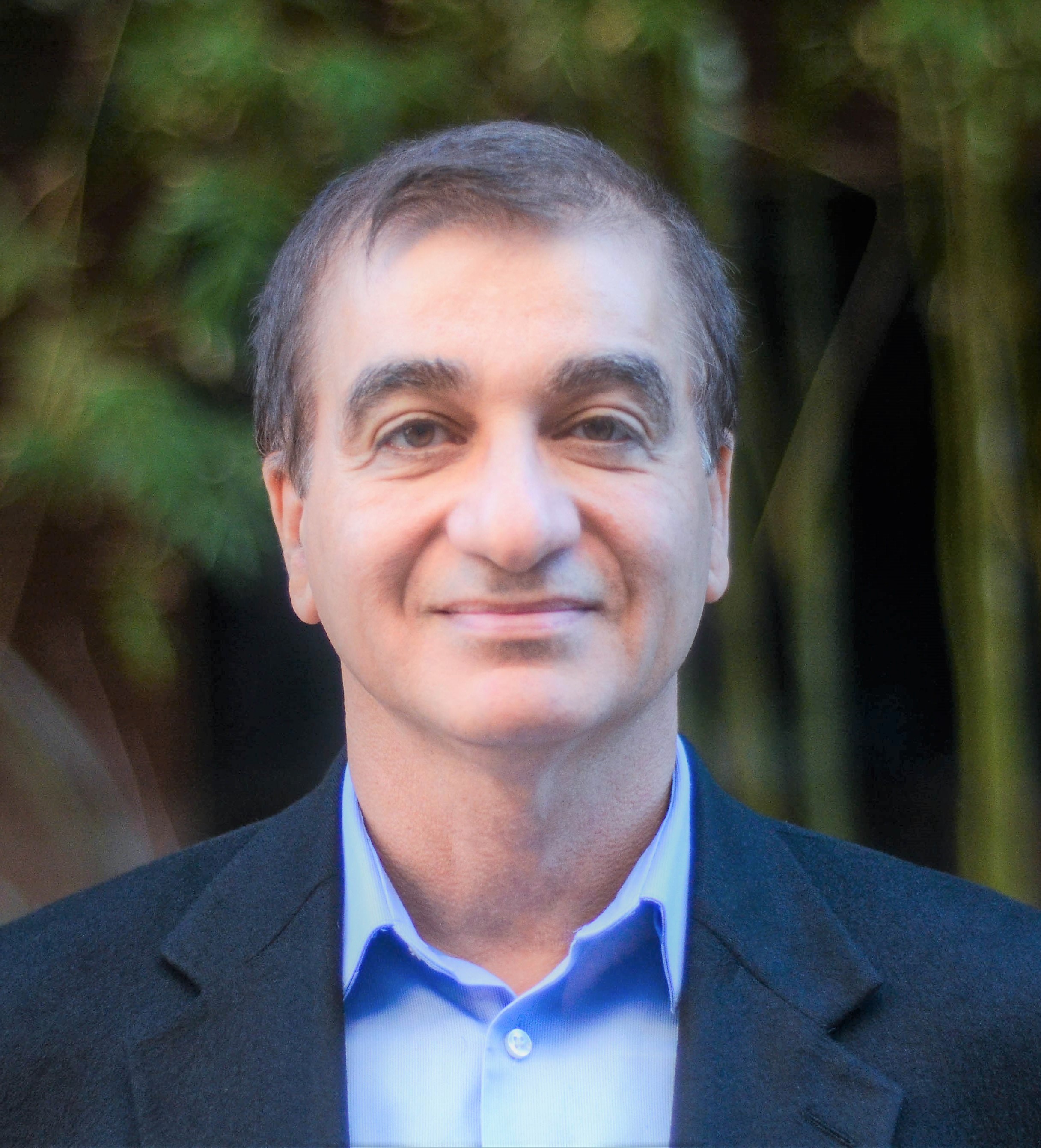 Massoud Pedram合作论文数Ming Hsieh Department of Electrical and Computer Engineering, Viterbi School of Engineering, University of Southern California7
 Behrouz Afzal合作论文数6
 Hamid Mahmoodi合作论文数School of Engineering, College of Science and Engineering, San Francisco State University5Bahareh Seyedzadeh Sany合作论文数3Saeed Mohammadi合作论文数3
 Hassan Afzali-Kusha合作论文数3
 Roohollah Yarmand合作论文数3
 Hossein Aghababa合作论文数School of Electrical and Computer Engineering, University of Tehran3m saremi合作论文数2
 Reza Asadpour合作论文数2
 Nima Eslami合作论文数Fac Elect Engn, Shahid Beheshti Univ2
 Deniz Najafi合作论文数2
 Erfan Shakouri合作论文数2
 Kolsoom Mehrabi合作论文数Dept Commun & Elect, Shiraz Univ2
 Omid Akbari合作论文数College of Engineering, University of Tehran2
 Pooya Torkzadeh合作论文数2
 Saeed Zeinolabedinzadeh合作论文数Sch. of Electr. & Comput. Eng., N.W. Georgia Tech;c;Sch. of Electr. & Comput. Eng., N.W. Georgia Tech2
 Mehdi Saremi合作论文数School of Electrical and Computer Engineering, University of Tehran2
 Massoud Dousti合作论文数Department of Electrical Engineering, Science and Research Branch, Islamic Azad University2
 Masoud Rostami合作论文数Rice University2
 Mohammad Hossein Moaiyeri合作论文数Faculty of Electrical and Computer Engineering, Shahid Beheshti University2
 Farzan Jazaeri合作论文数1Mohammad Ghanatabadi合作论文数1Mohammad Ansari合作论文数1Bahareh Vakili合作论文数1
 Samaneh Soleimani-Amiri合作论文数Department of Electrical and Computer Engineering, Babol Noshirvani University of Technology1
 Mohammad Chahardori合作论文数School of EECS, Washington State University, Pullman, Washington, USA1
 Sina Sayyah Ensan合作论文数School of EECS, Pennsylvania State University, Univeristy Park, USA1
 Nader Sehatbakhsh合作论文数Electrical and Computer Engineering Department, School of Engineering, University of California, Los Angeles1
 Mahdi Moradinasab合作论文数Sch. of Electr. & Comput. Eng., Univ. of Tehran;c;Sch. of Electr. & Comput. Eng., Univ. of Tehran1
 Moein Kianpour合作论文数Department of Electrical Engineering, Islamic Azad University1
 Mohsen Asad合作论文数1
 Jawad Faiz合作论文数School of Electrical and Computer Engineering, College of Engineering, University of Tehran1
 Zainalabedin Navabi合作论文数Worcester Polytechnic Institute1
 B. Forouzandeh合作论文数1
 Majid Mohammadi合作论文数1
 Reza Sabbaghi-Nadooshan合作论文数Department of Electrical Engineering, Central Tehran Branch, Islamic Azad University;School of Computer Science, Institute for Research in Fundamental Sciences1
 Morteza Fathipour合作论文数School of Electrical&Computer Engineering, University of Tehran1S. Hessabi合作论文数Department of Computer Engineering
Sharif University of Technology1Vahid Moalemi合作论文数University of Tehran1
Morteza Fathipour合作论文数School of Electrical&Computer Engineering, University of Tehran1S. Hessabi合作论文数Department of Computer Engineering
Sharif University of Technology1Vahid Moalemi合作论文数University of Tehran1




