As modern GPUs integrate massive processing elements and limited memories on-chip, the efficiency of using their scratchpad memories becomes important for performance and energy. To meet bandwidth requirement of simultaneously accessing of a thread array, multi-bank design, dividing a scratchpad memory into equally-sized memory modules, are widely used. However, the complex access patterns in real-world applications can cause the bank conflicts which comes from different threads accessing the same bank at the same time, and the conflicts hinder the performance sharply. A mapping function is a method that redistributes the accesses according to access addresses. To reduce bank conflicts some scratchpad memory mapping functions are exploited, such as XOR based hash functions and configurable functions. In this paper, we propose an adaptive mapping function, which can dynamically select a suitable mapping function for applications based on the statistics of first block executing. The experimental results show that 94.8 percent bank conflicts reduced and 1.235× performance improved for 17 benchmarks on GPGPU-sim, a Fermi-like simulator.
In this paper, we propose an optimized bitonic sorting architecture and a hybrid sorting architecture for addressing the sorting problem of successive cancellation list decoders for polar codes. Since half of the 2L metrics are already sorted, lots of redundant sorting operations can be deleted. According to this property and the characteristics of the sorting network, we put forward several optimization strategies to reduce the compare-and-exchange units and the pipeline depths. For the list size L ≤ 32, the synthesis results show that the area of proposed hybrid sorter is at least 22% smaller than existing sorters, and the latency is at least 25% smaller.
This paper describes the application space exploration of a heterogeneous system with reconfigurable fabrics. The system is built around four reconfigurable engines and four digital signal processors (DSPs) that make it suitable for intensive computing kernel acceleration and complex control tasks. The system is geared toward high precision radar digital signal processing, and the reconfigurable engines are featuring the same structure to obtain high throughput by executing different tasks efficiently. Performance of the system is evaluated from measurements performed on a CMOS 40nm prototype. In order to characterize the application of the system, a complex real-life task is adopted, the results show that it can obtain a high throughput of 32.12Mpps and desirable precision.
Thermal sensor noise has great impact on the efficiency and effectiveness of a dynamic thermal management (DTM) strategy. Conventional reactive thermal management techniques suffer significant performance degradation due to the pessimistic reaction. In this paper, to address the problem of forecasting temperatures based on noisy thermal readings, we propose a Kalman predictor based runtime thermal prediction scheme, which can predict temperatures N step ahead. An activity-based power model for 3D NoC power estimation is also proposed; the model is an essential prerequisite of accurate temperature predictions. Besides that, we propose a distributed multi-input single-output (MISO) thermal model for 3D NoC systems, which reduces the computational complexity of temperature updating from m2 to m compared with the centralized multi-input multi-output (MIMO) model for the system with m units. The experimental results show that the proposed prediction scheme reduces the mean absolute error (MAE) by 42.8%-72.6% compared with the auto-regressive (AR) based prediction scheme.
In this paper, we propose a high performance matrix inversion implementation on a reconfigurable application specific processor. Our implementation can accelerate variable order matrix inversion ranging from 4 to 144. We adopt LU decomposition to reduce the computation complexity and a pivoting operation to ensure the stability. In order to get higher performance within the limited resources, parallel computing and time-sharing multiplexing are employed. The chip testing results show that our implementation improve the performance of inversion efficiently. The highest parallel speed-up ratio can achieve 3 times, and the execution time of a 144×144 matrix inversion is 4.07ms.
This paper presents an efficient architecture for performing 128 points to 1M points Fast Fourier Transformation (FFT) based on mixed radix-2/4/8 butterfly unit. The proposed FFT architecture reduces the computation cost by taking the advantage of the radix-8 FFT algorithm while remaining compatible with sequences whose data length is an integral power of 2. Further optimizations for reconfigurable application specified processor are developed. First, we propose a separated radix-2/4/8 butterfly unit which is more flexible than an entire radix-2/4/8 butterfly unit; second, for the sequences longer than 256K points, an efficient 2-epoch FFT solution is realized. This FFT architecture is implemented in a reconfigurable application specified processor. The computation time of our architecture is 676 us and 14.8ms for 128K and 1M points FFTs respectively.
To meet the increasing demand of large bandwidth and high throughput in modern radar system, we proposed a reconfigurable application specified processor (RASP) according to the feature of radar digital signal processing applications. RASP is a reconfigurable coprocessor based on hierarchical floating-point operation elements that is capable of executing a set of fundamental subalgorithms, take these subalgorithms as the minimal task node can improve the computational efficiency tremendously. The experimental results show that the processor performance exceeds TI state-of-the-art DSP by 1.05× to 3.22×. Our reconfigurable processor can be integrated into customizable radar systems, it was fabricated with TMSC 40 nm CMOS process and has an area of 19.2 mm2.
This paper presents an efficient architecture for computing 16 points to 1M points FFT( Fast Fourier Transformation) with a new FFT architecture based on mixed radix 2/4/8 butterfly unit. Taking advantage of the radix-8 FFT algorithm the proposed FFT architecture reduced the computation level while remaining compatible with sequences whose source data length is 2(n). Furthermore, some optimizations for reconfigurable application specified processor is developed. First, we propose a separated radix 2/4/8 butterfly unit which is more flexible than an entire radix 2/4/8 butterfly unit; Second, for the sequences longer than 128k points, an efficient 2D FFT computation solution is proposed. This FFT architecture is implemented in a prototype chip of reconfigurable application specified processor. Our architecture requires only 676 us and 7.4 ms for 128k points FFT and 1M points FFT respectively. Compared to the existing DSP processor GPGPU, the proposed performance approach improved in different degrees.
Through Silicon Vias (TSVs) based 3D Network on Chip (NoC) is a promising communication platform solution for future multicore systems. Due to the cost in terms of yield, chip area and design complexity, minimizing the number of TSVs in 3D integrated circuits has become an important design issue. In this paper, we present the circuit design of the proposed lateral asynchronous and vertical synchronous (LAVS) 3D NoC with double pumped vertical links and evaluate the area overhead, the die cost and the network performance of the scheme. Experiment shows the proposed scheme reduces overall router silicon area by 39.8%, and reduces the die cost by 20% for 3D NoC with 64 nodes each layer, and improves the ratio between performance and area by 16.8%.
Welcome to the WIT Press eLibrary - the home of the Transactions of the Wessex Institute collection, providing on-line access to papers presented at the Institute's prestigious international conferences and from its State-of-the-Art in Science & Engineering publications.
3D chip multi-processors (3D CMPs) combine the advantages of 3D integration and the parallelism of CMPs, which are emerging as active research topics in VLSI and multi-core computer architecture communities. One significant potentiality of 3D CMPs is to exploit the diversity of integration processes and high volume of vertical TSV bandwidth to mitigate the well-known “Memory Wall” problem. Meanwhile, the 3D integration techniques are under the severe thermal, manufacture yield and cost constraints. Research on 3D stacking memory hierarchy explores the high performance and power/thermal efficient memory architectures for 3D CMPs. The micro-architectures of memories can be designed in the 3D integrated circuit context and integrated into 3D CMPs. This paper surveys the design of memory architectures for 3D CMPs. We summarize current research into two categories: stacking cache-only architectures and stacking main memory architectures for 3D CMPs. The representative works are reviewed and the remaining opportunities and challenges are discussed to guide the future research in this emerging area.
 Hongbing Pan (潘红兵)合作论文数School of Electronic Science and Engineering, Nanjing University7
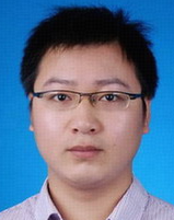 Jun Lin (林军)合作论文数School of Electronic Science and Engineering, Nanjing University5
 Fan Feng (冯凡)合作论文数College of Mechanical Engineering and Applied Electronics Technology, Beijing University of Technology5
 Yuxiang FU (傅玉祥)合作论文数School of Integrated Circuits, Nanjing University3YuAng Zhang (张宇昂)合作论文数2Baoning Zhang合作论文数2
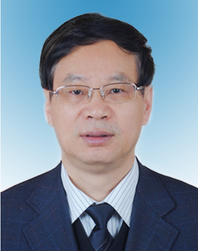 Guoqiang He (何国强)合作论文数Science and Technology on Combustion, Internal Flow and Thermal-structure Laboratory, Northwestern Polytechnical University2
 Jin Sha (沙金)合作论文数School of Electronic Science and Engineering, Nanjing University2dong yu合作论文数1
 Li Li (李丽)合作论文数Department of Microelectronics and Optoelectronics, School of Electronic Science and Engineering, Nanjing University1
 Kun Wang (王堃)合作论文数Department of Electrical and Computer Engineering, University of California, Los Angeles1
 Axel Jantsch合作论文数Institute of Computer Technology, Fakultat fir Elektrotechnik und Informationstechnik, TU Wien1
 Zhonghai Lu (鲁中海)合作论文数Division of Electronics and Embedded Systems, Department of Electrical Engineering, School of Electrical Engineering and Computer Science, KTH Royal Institute of Technology1
 Minglun Gao (高明伦)合作论文数Hefei University of Technology1




