An advanced structural and physical model of Intermediate Layer Dielectric (ILD) cracking in a planar gate under short-circuit (SC) conditions has been developed as a continuation of our previous studies. This approach utilizes an energy-based Rankine damage model, which is applied based on the mechanical properties of SiO2. The Rankine model has been seamlessly integrated into a comprehensive 2D electrothermal-metallurgical and elastoplastic-mechanical framework, which accounts for both the high-temperature rise and its return to its reference value during the cooling phase. In a novel approach, multiple repetitive mechanical cycles were simulated to evaluate the progression and rate of crack penetration, with variations in parameters such as pulse duration and damage model coefficients. This model illustrated the evolution of crack formation and direction during cycling, in alignment with the crack progression observed experimentally in microsections.
p-GaN gate HEMTs are highly attractive for power applications but exhibit complex reliability issues related to trapping effects and high-field stresses. Accurate investigation of these mechanisms requires a calibrated physical model able to reproduce the electrical behavior of the device. In this work, a TCAD fitting methodology for a commercial p-GaN HEMT is proposed. Unlike purely automated optimization techniques, the approach relies on a semi-empirical, experience-driven parameter adjustment strategy to achieve a physically consistent parameter set. Using the fitted model, a study of trapping parameters highlights the relevance of the capacitive marker $C_{\text {RSS }}\left(V_{\text {DS }}\right)$ for identifying the localization, nature, and density of active traps in hard-switching operation and reverse conduction operation conditions from experimental results.
Due to the poor quality of the silicon carbide / silicon dioxide interface realization and their thin gate oxide layer, SiC mosfets are more susceptible to charge-trapping mechanisms than silicon mosfets. These phenomena are amplified over time, resulting in decreased transistor performance and increased losses. To monitor this aging mechanism, an analog method is proposed to extract a newly discovered health indicator from the gate voltage (V-GS) waveform. This is accomplished by slowing down a specific turn-on using a dual-channel active gate driver. The online health monitoring method is then experimentally validated on a 1200 V-36 A SiC mosfet in both no-load and pulsewidth modulation conditions.
The authors proposed in-depth experimentation and physical analysis showing the extreme robustness capability of low-voltage GaN HEMT in single and repetitive short-circuit. A 2DEG pinch-off behavior is analyzed depending on VDS voltage and charges' trapping / de-trapping relaxation time. A new drain-gate leakage-current mechanism at turn-off is suggested to explain the ultimate thermal-runaway failure-mechanism.
The use of an active gate driver offers multiple advantages and enables the full exploitation of SiC MOSFETs in terms of both performance and reliability. This is particularly important given the specific gate-driving challenges associated with high-voltage SiC power MOSFETs. In the off-state, a negative gate bias induces high electric field stress across the gate oxide, potentially compromising device reliability. Conversely, a positive gate bias can result in excessive drain saturation current under short-circuit conditions. These conflicting requirements impose trade-offs that conventional two-level gate driver topologies cannot fully resolve. To address these limitations, this work presents a novel, Modular Multilevel Active Gate Driver (MMAGD), implemented as a single CMOS integrated circuit. The proposed MMAGD topology introduces new degrees of freedom for dynamic gate control, enabling optimized and adaptive driving of Wide Bandgap (WBG) power devices such as SiC MOSFETs. Experimental results validate the effectiveness of the circuit and demonstrate its potential to improve performance and reliability under demanding operating conditions.
For the first time in SiC MOSFETs, structural and physical modeling of the Intermediate-Layer-Dielectric (ILD) cracking in a planar gate under short-pulse short-circuit conditions is proposed. This approach employs an energy-based Rankine damage model, relying on the SiO2 mechanical properties. The Rankine model has been effectively integrated into a comprehensive 2D electrothermal-metallurgical and elastoplastic-mechanical model across a wide range of temperatures. Initial results enable the extraction of crack penetration depth from a single pulse, paving the way for estimating the average number of critical cycles leading to a potentially complete destructive ILD fracture.
To address their fragility and limitations in high-reliability, safety-critical applications, especially in future aeronautic on-board power systems, SiC MOSFETs are increasingly paired with smart gate drivers. These drivers provide health diagnostics, dv/dt control to reduce losses and EMI, and integrated fault detection. With newer generations, SiC MOSFETs demonstrate increasingly shorter short-circuit withstand times. A multi-channel parallel gate driver with extensive fault detection and gate-oxide integrity monitoring, based on gate-source voltage monitoring is proposed. On commercial 1200 V Gen. 3 SiC MOSFETs, Hard Switching Faults and Faults Under Load are detected within 890 ns and 235 ns, respectively. Gate-Oxide cracks are identified before controllability is compromised, and the robustness of this detection method is experimentally validated.
As a follow-up to our previous work, the 2D transient Multiphysics electrothermal-mechanical and metallurgical model of a 1.2kV-80m. gate-planar SiC MOSFET power chip in a single FEM software, created previously by the authors, has been developed. This model aims to quantify the short-circuit (SC) critical time and energy density of attaining the local dielectric interlayer (ILD) strength and the Al source-metal solidus-liquidus phase transition at elevated temperatures. The novelty of this extended model is considering non-linear electrothermal and elastoplastic material property laws over a wide range of temperatures. Repetitive experimental SC events were carried out to verify the gate-aging occurrence in accordance with the critical values extracted from the proposed model.
This study focuses on the drain-source breakdown voltage (V BR ) of 100 V commercial p-GaN transistors. By presenting V BR values, showcasing device dispersion, and employing failure analysis (FA), we explore various physical degradation mechanisms. Investigating the degradation process from origin to defect manifestation enhances our understanding of GaN transistor limitations. Additionally, the paper highlights the adaptation of FA methodology based on defect nature, providing valuable insights for semiconductor device reliability improvement.
New and original medium power multi-terminal SiC monolithic converter architectures are investigated with vertical switching cells based on SiC JBS diodes and VDMOS transistors. 2D TCAD and mixed-mode Sentaurus™ simulations are performed to optimize switching structures as Buck, Boost, H-bridge high-side row chip common drain-type and low-side row chip common source-type. The proper operation in the turn-on and turn-off of each cell is also studied and validated. To fabricate these new monolithic integrated architectures, two main technological bricks have been developed, for vertical insulation and the integration of a top Ni metal via. To achieve the vertical insulation deep trenches are necessary combining dry plasma and wet KOH electrochemical etching through the thick N+ substrate.
SiC power MOSFETs, compared to their Si counterparts, still lack maturity, hindering their adoption in aeronautical applications. Consequently, there is a growing need for the development of smart gate drivers with built-in functions like health monitoring. Reducing failures and downtime in power converters relies on an early detection of component ageing. However, assessing reliably the health condition of power transistors in PWM operation remains a challenge. In this perspective, a non-invasive strategy is proposed. This approach aims to determine precisely and accurately the health state of the gate oxide of a SiC power MOSFET. It uses a dual-channel gate driver to trigger a slow turn-on event and clean switching measurement within a PWM frame. This method involves an online tracking of oxide ageing, or charge-trapping indicators present in the gate signal waveform.
This paper presents a methodology for the physical analysis of defects on p-GaN power HEMTs that have been electrically stressed under DC surge or voltage switching stresses. The methodology includes a backside approach for sample preparation and defect localization. It is crucial to adapt the preparation process according to the position of the defect in the device structure (including metallurgy, dielectric layers, epitaxy, etc.), which depends on the type of stress applied. In our study of the reliability of the transistor under increased electrical stress in lifetime operation mode, failure analysis is used to identify the weakest areas in the design with respect to the type of stress applied. This paper presents a failure analysis consisting of techniques such as electrical characterization, photon emission microscopy and lock-in thermography for defect localization, focused ion beam slice and view, transmission electron microscopy analysis, and frontside conductive atomic force microscopy after immersion in hydrofluoric acid.
Existing literature has primarily focused on using gate signals for short-circuit type I detection (Hard Switch Fault, HSF). However, an unaddressed aspect remains in detecting the short-circuit type II (Fault Under Load, FUL). This article introduces a Gate-Driver (GD) IC with a fully integrated approach for the FUL detection. This solution strategically uses the gate current copy, enabling ultra-fast FUL detection. Experimental results demonstrate reliable fast short-circuit detections for power modules, in less than 100ns. This IC is fabricated using NXP Semiconductors' high-voltage SMARTMOS10 130nm CMOS SOI technology.
This article proposes a generic and complete electro-thermal 4H-SiC physical Mosfet model. Static and transient in hard short-circuit operation behaviors are successfully performed using 2D Comsol™ software. Influence of fixed charges and traps at the 4H-SiC/SiO2 interface has been highlighted, both for static and transient. An additional mobility coefficient through Arora's mobility model was then suggested to fully fit the transient model in hard short-circuit operation.
A full monolithic integration in multi-terminal SiC dies of a generic H-bridge power converter (800V/10A) consisting of dual N-type vertical MOSFET switches within only two multi-terminal chips is proposed. Innovative two multi-terminal monolithic power SiC-chips are introduced and studied by 2D Sentaurus™ simulations. The first one integrates the high-side row switches of the bridge and the second one integrates the low-side row switches. Static and dynamic operating modes were validated through 2D-Mixed-Mode simulations. Main new process bricks allowing back-side insulating trenches based on plasma combined with photo-electrochemical etching are experimentally evaluated for the first time on power device SiC wafer.
This paper describes a backside approach methodology for sample preparation, fault localization and physical defect analysis on p-GaN power HEMT electrically stressed in DC voltage surge and AC switching mode. The paper will show that preparation must be adapted according to the defect position (metallurgy, dielectric layers, epitaxy, etc.) which depends on the type of stress applied. In our life-operation mode amplified electrical stress reliability study, the failure analysis will help us to reveal the weakest parts of the transistor design in relation to the type of applied stress. The failure analysis presented in this paper is composed of electrical characterization, defect localization with PEM and LIT, FIB Slice&View, TEM analysis and frontside conductive AFM after a deep HF.
For the first time, a complete 2D transient multiphysics electro-thermo-mechanical and metallurgical model of a 1.2 kV-80m omega gate-planar SiC MOSFET power chip has been developed in a single FEM software. This model is used to quantify the short-circuit critical time and energy density with respect to the local SiO2 interlayer strength at high temperatures and the Al source-metal solidus-liquidus phase transition temperature. Repetitive experimental short-circuits were conducted to confirm the gate-aging existence in coherence with the critical values extracted from the proposed model.
The main factor still hindering a wide industrial adoption of SiC power MOSFETs is essentially a global reduced ruggedness in comparison to their Si counterparts. The proposed gate driving architecture leverages fault-induced gate voltage disturbances and enhances them to facilitate their detection through two dedicated commutated gate resistors. This approach combines switching dynamics and enhanced ON-state fault sensibility. This architecture, affording innovative short-circuits and overload detections, as well as gate-oxide integrity monitoring, was validated on a 600 V short-circuit power test bench using commercial 1200 V/36 A SiC MOSFETs.
 Abdelhakim Bourennane合作论文数33
 Marc Cousineau合作论文数Lab. Plasma et Conversion d'Energie, Univ. de Toulouse;c;Lab. Plasma et Conversion d'Energie, Univ. de Toulouse19
 Thierry Meynard合作论文数Laboratoire Plasma et Conversion d'Energie, Centre National de la Recherche Scientifique19
 Jean-Marc Blaquière合作论文数19
 Nicolas Rouger合作论文数19
 Emmanuel Sarraute合作论文数18Sebastien Vinnac合作论文数15
 F. Boige合作论文数Gamma Technologies15Jean-Louis Sanchez合作论文数11Adem Lale合作论文数11
 François Forest合作论文数11
 Yazan Barazi合作论文数Correspondence to: 2 rue Charles Camichel Toulouse, BP7122 – 31071 Toulouse Cedex 07, France.9
 Capy, F.合作论文数9Breil, M.合作论文数9
 David Trémouilles合作论文数CNRS, LAAS9
 Hubert Piquet合作论文数CNRS-INPT-UPS, Université de Toulouse9
 Gerald Guibaud合作论文数8
 Jeanpierre Laur合作论文数8
 Guillaume Gateau合作论文数Lab. d''Electrotech. et d''Electron. Ind., CNRS;c;Lab. d''Electrotech. et d''Electron. Ind., CNRS8
 Christophe Turpin合作论文数8
 Stephane Azzopardi合作论文数IXL – ENSEIRB8
 Stéphane Lefebvre合作论文数7
 Jean-Jacques Huselstein合作论文数7Nicolas Videau合作论文数6Mathis Picot-Digoix合作论文数6
 damien risaletto合作论文数6
 Linh Thuy Thi Pham合作论文数5
 Franck Mosser合作论文数5Henri Foch合作论文数5
 Plinio Bau合作论文数IRT Saint Exupery5Wadia Jouha合作论文数UPS, University of Toulouse5
 Nicolas Roux合作论文数5
 Alberto Castellazzi合作论文数Engineering Department, Kyoto University of Advanced Science5Thanh T. Le合作论文数Department of Molecular and Cellular Biochemistry, Ohio State University5
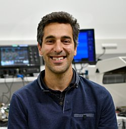 Bernardo Cougo合作论文数5
 Didier Flumian合作论文数5V. Chazal合作论文数4Matthew Bacchi合作论文数4J. -M. Blaquiere合作论文数4Baudesson, P.合作论文数4
 Amirouche Oumaziz合作论文数4
 Lucien Ghizzo合作论文数4Pierre Calmes合作论文数4
 Mustafa Shqair合作论文数4y cheron合作论文数4El khadiry, A.合作论文数4
 Sanchez, S.合作论文数4Austin, P.合作论文数4
 Bennani Ben Abdelghani, A.合作论文数4




