We present the first experimental machine learning (ML)-enabled Process-Technology Co-Optimization (PTCO) framework for optimizing 2D transition metal dichalcogenide (TMD) FET fabrication directly from statistically meaningful experimental data rather than pure simulation data. We first introduce a transition voltage metric, VTrans, to quantify the gate voltage required for off-to-on switching and reveal its direct correlation with subthreshold swing (SS), highlighting an overlooked switching characteristic that governs both off-state and on-state performance. By integrating automated metric extraction, multi-objective recipe ranking, and predictive modeling, our framework uncovers hidden process-performance correlations and predicts the performance of unexplored fabrication recipes from limited experimental data. Experimental validation shows close agreement with ML predictions, thus demonstrating the framework's ability to efficiently guide gate stack optimization through iterative experimental feedback.
Logic and memory transistors integrated with oxide semiconductors are promising for monolithic 3D systems that enable reconfigurable functionality and enhanced on-chip communication. However, challenges in controlling carrier mobility, carrier concentration, and defect density have hindered their deployment in advanced chip technologies. Here, we report a heterojunction oxide semiconductor channel approach that mitigates the interface/channel defect density and achieves field-effect mobility to >100 cm2/V.s, competitive with thin-film silicon channels. By engineering a bilayer oxide channel, we demonstrate a low-thermal-budget, ultra-scaled, memory-logic dual-mode ferroelectric transistor that exhibits a high on-state current of 800 µA/µm at Vd = 1 V, a positive threshold voltage, and excellent reliability with only 30 mV threshold shift after 5000s of gate-bias stress. Furthermore, it exhibits robust memory endurance exceeding 107 cycles and a fast ferroelectric read-after-write delay of 180 ns. TCAD simulation (Ginestra) reveals that performance improvement is attributed to the defect self-compensation effect in bilayer channel, which stabilizes disordered metal bonds and weakly bonded oxygen states. This work establishes a pathway towards reliable, high-performance oxide-based transistors, offering a scalable solution for next-generation low-power reconfigurable chips tailored for generative artificial intelligence.
The integration of dielectric inserts into hafnia-based ferroelectric stacks has emerged as a promising route to expand memory windows in ferroelectric NAND. However, the physical origin of the associated coercive voltage enhancement has remained unclear. Here, we resolve this long-standing question by demonstrating that coercive voltage enhancement originates from resistive voltage division between the ferroelectric and dielectric layers, governed primarily by leakage in both layers. Combining Preisach modeling, defect-based Ginestra simulations, and polarization switching experiments with external leaky dielectrics, we show that minimizing leakage in the dielectric layer - intrinsically through wide-bandgap, low-electron-affinity dielectrics or extrinsically by reducing defect densities - provides a universal design principle for coercive voltage control. Importantly, nucleation-limited switching kinetics remain unchanged across the heterostructures, confirming that the enhancement is driven by resistive voltage division rather than trap-assisted mechanisms. This discovery establishes a straightforward framework for engineering large memory windows using ferroelectric-dielectric heterostructures, thereby enabling multi-level (TLC/QLC) operation in 3D NAND. Beyond memory applications, our findings also explain the contrasting behaviors of fluorite- vs. perovskite-based ferroelectric-dielectric systems, offering fundamental guidance for interfacial materials design in next-generation electronic devices.
For the first time, this work presents a smart pixel design enabled by a tunable-capacitance ReRAM (TCReRAM) device. The fabricated Al/Ta/HfOx/Au TCReRAM, operated in deep-reset mode, provides up to 60% capacitance tunability over a voltage range relevant to pixel operation. This single nanoscale element can replace bulky in-pixel CG-tuning circuitry, enabling a simpler, scalable pixel with real-time scene-adaptive performance.
We investigate the impact of a monolithic 3-D (M3D) integration process-critical 400(degrees)C postprocessing forming gas annealing (FGA) on the electrical performance, reliability, and defect evolution of oxide-channel thin-film transistors (TFTs), combining systematic experiments with density-functional-theory (DFT)-based liquid-quench molecular-dynamics (MD) simulations. Indium tungsten oxide (IWO) TFTs are employed as a model system and encapsulated with a thin 3-nm Al2O3/3 nm HfO2 hybrid layer that effectively suppresses external hydrogen ingress. We reveal a nonmonotonic evolution of device behavior during FGA, governed by initial densification followed by partial crystallization. Short-duration FGA (10 min) induces channel densification and the formation of shallow, delocalized defect states, leading to pronounced positive bias temperature instability (PBTI) degradation and the emergence of a characteristic transfer-curve "kink." With prolonged annealing (>40 min), partial crystallization of the oxide channel occurs, stabilizing hydrogen in deep, localized defect states, suppressing hydrogen mobility, and restoring device reliability. As a result, the PBTI shift is reduced to 10.4 mV after 2000 s of stress, accompanied by complete elimination of the transfer-curve kink. These findings provide a mechanistic understanding of hydrogen-defect interactions during high-temperature postprocessing FGA and demonstrate that appropriate hydrogen-blocking encapsulation enables oxide-channel TFT integration without compromising electrical performance or reliability.
Bulk traps play a critical role in the reliability of GaN-based devices; however, existing characterization techniques are limited in their ability to simultaneously resolve trap energy, spatial location, and density. In this work, a redefined AC transconductance ($\mathbf{A C}-\boldsymbol{G}_{\boldsymbol{m}}$) characterization method is proposed for GaN MESFETs, extending the conventional MOSFET-based AC-$\boldsymbol{G}_{\boldsymbol{m}}$ framework to bulk trap analysis. A physical model based on Shockley-Read-Hall emission is developed to correlate frequency- and bias-dependent AC-$\boldsymbol{G}_{\boldsymbol{m}}$ dispersion with the spatial and energetic distributions of bulk traps. The method is applied to GaN MESFETs subjected to heavy-ion irradiation and off-state electrical stress, enabling reconstruction of threedimensional bulk trap distribution maps under different degradation conditions. TCAD simulations using the Ginestra™ tool show strong agreement with the experimental analysis, verifying the accuracy and robustness of the proposed method. This work demonstrates that the redefined AC-$\boldsymbol{G}_{\boldsymbol{m}}$ technique provides a reliable and complementary approach for depthresolved bulk trap characterization in GaN MESFETs.
This work reports back-end-of-line (BEOL) compatible, thin-film transistors (TFTs) with sub-10 nm tungsten-doped tin oxide (TWO) channels deposited by atomic layer deposition (ALD) at 150 ^∘C. TFTs with undoped SnO_x, undoped WO_x, and W-doped SnO_x channels with W concentrations of 5
We report a comprehensive study on memory window (MW) enhancement and retention loss (RL) in ferroelectric (FE) field effect transistors for NAND applications with a dielectric layer inserted within the FE film (next to the gate - GBL devices - or in the middle of the FE layer - TDL devices). Using a temperature-dependent modeling framework, we show that MW and RL properties are controlled respectively by carriers trapping into defects at the dielectric-FE interface and by its fragile balance with FE depolarization. While MW enhancement is achieved whenever the inserted dielectric layer is present, a robust retention is obtained only in TDL FEFETs, thanks to a stabilization of the trapped charge preventing FE depolarization. Simulation results clearly demonstrate that the fragile balance between above phenomena is ultimately controlled by the position of the dielectric layer, which determines i) the field redistribution within the stack, ii) the magnitude of charge de-trapping, and iii) the magnitude of the depolarization field. Our results provide critical guidelines for the improvement of FE 3D-NAND reliability.
We report a material-to-device co-optimization workflow based on multi-scale simulations applied to the endurance improvement of ferroelectric (FE) capacitors engineered with a WOx Oxygen (O) reservoir layer (ORL). Electrical data (on standard HZO FE devices), ab-initio modeling and device-level simulations are synergically used to unveil and identify the processes associated with the presence of the WOx ORL. The acquired know-how is then experimentally validated using HZO FE capacitors engineered with an interfacial WOx ORL that demonstrates enhanced endurance and suppressed trap generation rate.
Combining experimental methods and multi-scale modeling we untangled the mechanism underlying the dipole formation and captured their impact on reliability through Carrier Injection (CI) model for HKMG under negative stress voltages. Simulations unveil the existence of a trade-off between dipole-induced VFB shift and device reliability metrics (leakage, breakdown). We show that: i) Al diffusion scavenges interface layer (IL) inducing VO+ defects that increase gate leakage current; ii) IL scavenging increases with Al content; iii) stress-induced defects at HK play a major role in triggering breakdown. Finally, we show that 4A is the optimal Al dipole layer thickness which doesn't impact stack's integrity and device's reliability.
Endurance degradation in conventional Si-channel ferroelectric FETs (FEFETs) is predominantly governed by trap generation within the interfacial SiO2 (IL) layer, where elevated electric fields accelerate defect generation, leading to polarization screening and progressive memory window (MW) collapse. In this work, we demonstrate that using scavenging to thin the IL layer induces a sub-stoichiometric SiOx, with higher capacitance which dramatically improves the endurance characteristics of the FEFET. This IL engineering results in a redistribution of voltage and a new mode of FEFET failure driven by the underlying FE rather than the IL. This FE-driven degradation paradigm yields three critical advantages: (1) suppression of subthreshold slope (SS) deterioration by minimizing interface state buildup, (2) MW stability over extended cycling, as evidenced by a stable high-V-Th and low-V-Th states until FE breakdown, and (3) reduction in read-after-write latency due to faster de-trapping of traps in IL layer. We also demonstrate robust MW at 125 degrees C with 104 cycles endurance and low SS. Further, we quantify trap generation and electric fields in the IL and FE layers using Ginestra (TM) simulations. These findings establish an innovative and efficient pathway to high endurance, stable VTh FEFETs via the implementation of an IL engineering-driven control of ferroelectric degradation.
Bulk switching RRAM technologies have been developed to address nonidealities of filamentary RRAM for embedded compute-in-memory applications. However, high density 3D integration and scalability to nano regime have yet to be experimentally demonstrated. Here, we present a scalable, filament-free 3D 8-layer vertical bulk RRAM (b-RRAM) technology optimized for embedded compute-in-memory (CIM) applications. This forming-free device features reliable cycling, multi-level switching, and enhanced speed via hydrogen doping. Guided by multiscale device simulations to optimize the switching stack, we demonstrate 40x40 nm(2) b-RRAM cells with MO-level resistance and current nonlinearity, enabling accurate, energy-efficient matrix-vector multiplications (MVM) in selector-less crossbars. A hyperdimensional computing-based continual learning algorithm is implemented on 3D b-RRAM for edge AI tasks, achieving similar to 90% accuracy-comparable to high-precision floating-point (FP) baselines-while delivering substantial energy savings.
Memory window (MW) closure, read delay, and gate leakage are three key reliability challenges in ferroelectric (FE) field-effect transistors (FEFETs), all of which have traditionally been analyzed separately. In this work, we exploit dedicated experiments and device simulations to present a detailed study of these three mechanisms in Si-FEFETs with a 10nm layer of FE HZO. The results reveal critical insights into the interplay between trap generation and polarization switching (PS), and the correlation between MW closure, read delay, and leakage current. First, we show that trap generation is accelerated by PS and initially (up to 5x10(4) cycles) occurs mainly in the interfacial layer (IL). These PS induced traps are slow traps and are found to be responsible for both reduction in MW recovery with read delay and MW closure, demonstrating a strong correlation between the two mechanisms. Finally, we show that leakage current increase is controlled by the generation of HZO traps, which is triggered by internal field redistribution once IL is highly degraded (after MW closure). The engineering of FEFETs to minimize the formation of slow (de)trapping defects in the IL is essential to improve overall reliability of the FEFET device.
We report the experimental observation of discrete ferroelectric switching down to 0.475 nm x 0.475 nm in HfO2-based ferroelectrics using correlated STEM electron beam induced current (EBIC) imaging and nanoscale voltage pulsing. These high-resolution measurements reveal single-domain switching events characterized by abrupt, bi-state transitions with no intermediate polarization states. By mapping polarization-voltage behavior and switching kinetics across thousands of domains, we extract spatially resolved switching thresholds (E-min), switching speeds (t(sw)), and remanent polarization (2P(r)), uncovering robust scaling trends. Larger domains exhibit nearly twice the polarization and faster switching despite higher E-min, while smaller domains switch more slowly at the same field. Sub-domain imaging enables quantification of variation scaling: polarization variation increases linearly logarithmically with area, with inter-domain variation dominating intra-domain variation. Importantly, we show that multi-bit operation arises from the statistical distribution of domain-level switching-rather than partial polarization-enabling distinct and reliable states in devices as small as 0.01 mu m(2). These findings provide a foundational experimental framework for designing scalable, multibit ferroelectric memory based on grain- and domain-level heterogeneity.
We present novel back-end-of-line (BEOL) copper interconnect integration for advanced technology nodes using low-k dielectric dep, binary liner metal gapfill process, radical assisted annealing, chemical mechanical planarization (CMP) and selective metal cap. Unit process and metrology data, electrical tests, Time Dependent Dielectric Breakdown (TDDB) reliability, Electromigration (EM) reliability and circuit simulations confirm significant power-performance-area (PPA) gains for 2nm technology node and beyond.
We present a novel deuterium (D-2) plasma treatment process for interface passivation that leads to reliability improvement under a low thermal budget. Specifically, physics-based simulations revealed a marked enhancement of key reliability phenomena such as leakage current, Negative Bias Temperature Instability (NBTI) and Voltage-Dependent Dielectric Breakdown (VDDB), also confirmed by experiments. Furthermore, the plasma treatment process optimization is accelerated through a physical model based on the Ginestra (TM) simulation platform, which connects the process conditions to the defect passivation and the best device reliability.
Artificial intelligence (AI) continues to drive transformative advancements across various industries. The data-intensive nature of AI training (and inferencing) has resulted in the generation of unprecedented volumes of data with machine-generated content surpassing human-generated data by more than 100-fold in 2025. Efficiently managing this data influx necessitates advanced digital storage technologies. However, traditional NAND flash memory, which is critical for supporting data flows in AI systems—alongside high-bandwidth memory, for AI training—faces fundamental scaling limitations as it approaches the 1000-layer milestone, encompassing more than 40 trillion transistors. This article delves into the potential of hafnia-based ferroelectric materials as a breakthrough solution to these challenges. Recent advancements indicate that the intrinsic limitations of ferroelectric field-effect transistors (FEFETs) can be mitigated through material and device-level engineering. These advancements enable FEFETs to meet the stringent density, reliability, and scalability requirements of future three-dimensional NAND technology. The role of ferroelectrics in addressing NAND scaling challenges and expanding storage capabilities presents a promising avenue for meeting the storage demands of the AI-driven era.
We study positive bias temperature instability (PBTI) in a dual-gated (DG) indium tin oxide (ITO) FET at room temperature (RT), 85 degrees C and 125 degrees C. We report record low threshold voltage shift, Delta V-th similar to -37.8 mV for top gate stress (2 V) at 125 degrees C. At higher temperatures, Delta V-th is reduced and V-th recovery is slower than at RT under identical stress. Simulations show elevated temperatures anneal shallow traps and activate deep-level traps, but these effects are temporary. These observations question the validity of elevated temperature accelerated reliability testing for ITO transistors, as it may not reflect long-term AOS device instability.
For the first time, we demonstrate that introducing an interfacial WO3 layer in ultra-thin ferroelectric Hf0.5Zr0.5O2 (HZO) capacitors improves endurance by 1000× at 125°C. It dramatically slows the degradation of write endurance with increasing temperature, leading to record-high endurance in a 5 nm HZO capacitor at elevated temperatures: 109 cycles at 85°C and 108 cycles at 125°C as well as >1012 cycles at 25°C -all for complete polarization switching $\left(2 P_r \approx 40 \mu \mathrm{C} / \text{cm}^2\right)$. Trap densities extracted from temperature- and cycling-dependent leakage currents show that the Oxygen vacancy (Vo) generation in HZO with cycling is significantly reduced in the presence of the WO3 layer. This is due to Oxygen (O) ion migration into HZO from WO3 during write pulses, which is favored by the asymmetric HZO/ WO3 diffusion barrier (as calculated by Density Functional Theory-based models). Since this prevents back diffusion of O ions from HZO into WO3, there is a net migration of O ions into HZO with continued cycling, partially healing cycling-induced Vo generation. This is a thermally activated self-healing process that becomes more efficient at elevated temperatures, thereby explaining our experimental observations. This concept can be useful for ferroelectric memories (FE-RAMs and -FETs) in emerging 3-D memory-on-logic architectures, where rising temperatures with increasing number of stacked dies is a major challenge.
 Luca Larcher合作论文数Dipartimento di Scienze e Metodi dell'Ingegneria, Università degli Studi di Modena e Reggio Emilia14
 Andrea Padovani合作论文数MDLab, Università di Modena e Reggio Emilia12
 Jack Lee合作论文数Chandra Department of Electrical and Computer Engineering, Cockrell School ofEngineering, The University of Texas at Austin10
 Feng Zhu合作论文数Shenyang Institute of Automation, China
Chinese Academy of Sciences, China
Chinese Academy of Sciences, Beijing, P.R.China
9
Feng Zhu合作论文数Shenyang Institute of Automation, China
Chinese Academy of Sciences, China
Chinese Academy of Sciences, Beijing, P.R.China
9 Yoshio Nishi合作论文数Department of Electrical Engineering, Stanford University8
 Krishna Saraswat合作论文数School of Engineering, Stanford University;Department of Electrical Engineering, Stanford University8
 Asif Khan合作论文数School of Electrical and Computer Engineering, College of Engineering, Georgia Institute of Technologygy8
 Manhong Zhang合作论文数8
 Tackhwi Lee合作论文数7
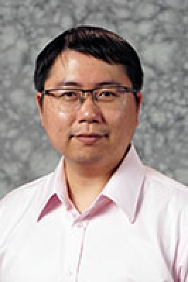 Shimeng Yu合作论文数Laboratory for Emerging Devices and Circuits, Georgia Institute of Technology;School of Electrical and Computer Engineering, Georgia Institute of Technology7
 Daewon Ha合作论文数6
 Masaharu Kobayashi合作论文数Institute of Industrial Science, University of Tokyo;Department of Informatics and Electronics, University of Tokyo;Rapidus Corporation6Chinsung Park合作论文数5xianmin tang合作论文数5
 Saurabh Chopra合作论文数Dept. of Electr. & Comput. Eng., Clemson Univ.;c;Dept. of Electr. & Comput. Eng., Clemson Univ.5
 Suman Datta合作论文数School of Electrical and Computer Engineering, College of Engineering, Georgia Institute of Technology;School of Materials Science and Engineering, Georgia Institute of Technology5
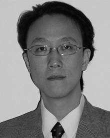 Chang Yong Kang合作论文数5
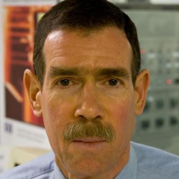 Theodore Kamins合作论文数Department of Electrical Engineering, Stanford University;Hansen Experimental Physics Laboratory, Stanford University5
 Jianshe Tang合作论文数5
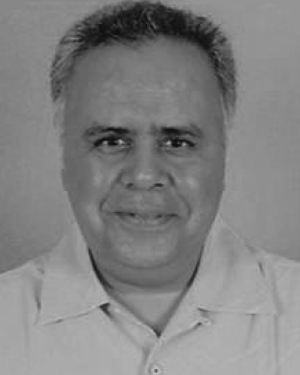 Mehul Naik合作论文数5
 Se Jong Rhee合作论文数5Y. Nishi合作论文数4B. Adams合作论文数4Alexander Jansen合作论文数4
 Hyoungsub Kim合作论文数4
 Ashish Pal合作论文数Applied Materials4El Mehdi Bazizi合作论文数4
 Changhwan Choi (崔暢桓)合作论文数Nano Electronic Devices & Materials Laboratory, Hanyang University;Division of Materials Science and Engineering, Hanyang University;Division of Nanoscale Semiconductor Engineering, Hanyang University;Research Institute of Industrial Materials Technology, Hanyang University4Hyosun Kim合作论文数Technical University of Braunschweig4
 Peter B. Griffin合作论文数4Mengkun Tian合作论文数School of Materials Science and Engineering, Central South University4
 Zhebo Chen合作论文数Dept Chem Engn, Stanford Univ4i j ok合作论文数3Sree Kesapragada合作论文数3Sidney Huey合作论文数3S. Moffatt合作论文数3Andrea Palmieri合作论文数3luping yu合作论文数3Vinod Reddy合作论文数3
 Nashrah Afroze合作论文数Dept Elect & Elect Engn, Khulna Univ Engn & Technol3max gage合作论文数3
 Jim Plummer合作论文数Department of Electrical Engineering, Stanford University3Jia Feng合作论文数3
 Andrew Poon合作论文数3
 S. Krishnan合作论文数Department of Computer Science;University of North Carolina3
 Federico Nardi合作论文数Dipartimento di Elettronica e Informazione and the Italian Universities Nanoelectronics Team (IU.NET),, Politecnico di Milano3
 James P. Mcvittie合作论文数stanford university3
 Shu-Lu Chen合作论文数3
 Injo Ok合作论文数3




