MOSFETs built in a thin layer of as-deposited, small-grain LPCVD polysilicon offer an attractive alternative to the beam recrystallized SOI MOSFETs because of its simple process and low cost. The inherently inferior performance of polysilicon MOSFET can be improved by the grain boundary passivation in hydrogen plasma. The device characteristics of n-channel and p-channel polysilicon MOSFETs are compared before and after the hydrogen passivation. Dramatic improve-ment of drive current and curtailment of leakage current has been observed after the passivation. The anomalous leakage current has been observed and is attributed to the soft breakdown of the drain junction.
The effects of the oxygen dose on the microstructure and the dielectric properties of the buried oxide in oxygen implanted silicon-on-insulator (SOI) structures have been studied. Cross-sectional transmission electron microscopy analyses show that the density of oxygen precipitates at the silicon/buried-oxide interface increases with a decreasing oxygen dose when identical annealing processes are employed. Annealing studies reveal that 1275 °C anneals annihilate the oxygen precipitates. A longer annealing time is required to achieve an oxygen-precipitate-free silicon layer in an SOI substrate implanted with a lower oxygen dose. The inverse relationship between oxygen content in the silicon film and oxygen dose is attributed to the redistribution of oxygen during implantation. In the oxygen dose range studied, the thickness and the breakdown voltage of the buried oxide layer increase with increasing oxygen dose. Higher postimplant annealing temperature improves the isolation properties of the buried oxide layer.
The effects of implant dose and postimplant annealing treatment on the microstructure of nitrogen-implanted silicon-on-insulator were studied by cross-sectional transmission electron microscopy techniques. In the lower dose case (0.75×10¹⁸/cm2) an amorphous silicon layer forms after implantation. Annealing at 1200 °C or higher results in a buried polycrystalline α-Si3N4 layer containing many randomly oriented silicon particles. Higher dose implantation results in an amorphous silicon-nitride layer. A porous layer also forms in the middle of the amorphous layer if the implant dose is 1.2×10¹⁸/cm2 or higher. The crystallization of the amorphous layer in the higher dose cases is shown to happen in two steps. In the first step nucleation and growth of α-Si3N4 grains occur in the amorphous nitride region to form a spherulitic polycrystalline structure. The second step is the cellular growth of the spherulitic nitride grains into the crystalline silicon regions. Silicon particles are trapped at the cell walls as the cellular reaction advances. These particles are conglomerated and sphereodized but retain the same orientation as the substrate silicon at higher temperatures. The quality of the top silicon film is excellent after annealing at 1200 °C or higher, irrespective of the implant dose.
The microstructure of buried oxide silicon-on-insulator (SOI) annealed in the temperature range of 1150–1300 °C was examined. The microstructure of the buried oxide SOI was improved by increasing the annealing temperature. The minimum channeling yield of the top silicon layer in 1250 °C annealed SOI measured by Rutherford backscattering and channeling analysis is 5% which is comparable to unprocessed bulk single crystal material. This is further verified by the cross-sectional transmission electron microscopy observation of the precipitate-free top silicon layer with low dislocation density. The improvement in the microstructure is attributed to the dissolution of oxygen precipitates and oxygen outdiffusion during high-temperature annealing.
Polysilicon transistors offer the first entry into 3-dimensional ICs. This paper reviews some process and device considerations in using these devices in VLSI environments. The process issues include the choice of polysilicon grain size, layer thickness, doping, and methods of grain boundary passivation. The device considerations are closely related to the effects of grain boundaries in modifying the device characteristics. Three specific application examples are reviewed. It is concluded that polysilicon transistors offer new possibilities to enhance the performance of bulk technologies without resorting to any recrystallization techniques.
Building on nearly two decades of reported results for MOSFET's fabricated in small-grain polycrystalline silicon, a design methodology is developed that yields devices which have low threshold voltage, high drive current, low leakage current, tight parameteric control, and reduced topology, while requiring no nonstandard materials, processes, and tools. Design criteria and device performance are discussed, grain boundary characterization techniques are described, technological issues pertinent to VLSI implementation are investigated, and long-term device reliability is studied. The potential applications of the polysilicon MOSFET's in high-density dRAM and sRAM are explored. The successful implementation of an experimental stacked CMOS 64K static RAM proves the utility of these devices for three-dimensional integration in a VLSI environment.
Using self-aligned and non-self-aligned stacked CMOS technologies experimental 8K × 8-bit static random-access memories (SRAM'S) have been fabricated. Hydrogen passivation has been used to improve the performance of polysilicon devices. An 8K × 8-bit SRAM using non-self-aligned memory cells and employing a CW argon laser to anneal the second (active) polysilicon layer has also been fabricated. The...
The effects of post implantation annealing on the properties of buried oxide silicon-on-insulator (SOI) substrates in the temperature range of 1150°C to 1300°C have been studied. Microstructural analyses showed that the crystallinity of the top silicon layer was improved at higher annealing temperature. Lower thermal donor generation at 450°C was observed in SOI annealed at higher temperature. The improvement in microstructure and lower thermal donor generation were correlated to the lower oxygen concentration in the top silicon film.
Buried nitride silicon-on-insulator (SOI) structures have been fabricated using the technique of nitrogen ion implantation. The crystallinity of the top silicon film was found to be exceptionally good. The minimum channeling yield, xmin, was better than 3%. This is comparable to the value observed for single crystal silicon. The buried insulator formed during the anneals has been identified as polycrystalline α-Si3N4 with numerous silicon inclusions. This nitride, however, has been found to remain amorphous in regions at the center of the implant where the nitrogen concentration exceeds the stoichiometric level of Si3N4. Nitrogen donor formation in the top silicon layer has also been observed.
Silicon-on-Insulator (SOI) technologies are becoming more important as CMOS becomes the preferred technology for VLSI. The progress of the three most actively researched SOI technologies, beam-recrystallized SOI, implanted buried oxide and Full Isolation by Porous Oxidized Silicon will be summarized in this paper.
Sillcon-on-Insulator (SOI) technologies are becoming more important as CMOS becomes the preferred technology for VLSI. The progress of the three most actively researched SOI technologies, beam-recrystallized SOI, implanted buried oxide and Full Isolation by Porous Oxidized Silicon will be summarized in this paper.
A silicon-on-insulator (SOI) material structure can be produced by the formation of a buried oxide layer beneath the surface of a silicon wafer by the implantation of oxygen ions. The typical fluence required is on the order of 1.3×1018 cm-2 of molecular oxygen at 300 keV. A 0.5 μm thick oxide layer is formed buried beneath a 0.12 μm thick layer of silicon. The top silicon layer is recrystallized by a high temperature anneal after the implantation. Large scale integrated circuits with excellent performance have been fabricated in epitaxial layers grown on this material.
High dose oxygen ion implantation has been used to form a buried oxide layer in Czochralski grown silicon. Wafers were implanted with 300 keV O2+ to a total dose of 1.32 × 10¹⁸ ions cm-2. A 0.5 m thick SiO2 layer is formed beneath a 0.17 μm thick top Si layer. Epitaxial films were grown on both annealed and unannealed wafers. Samples were subsequently annealed at 1150°C for times from 10 to 240 minutes in either Ar or N2. The highest quality epitaxial layers were obtained with substrates that were annealed after implantation, but prior to epitaxial growth for 2 hrs at 1150°C followed by 4 hrs at 1150°C after epitaxial growth. RBS channeling shows that the top 300 nm of these films have <110> channel backscattering yields lower than any SOI produced to date. The buried oxide plus epitaxial process is a leading candidate for VLSI applications.
High dose oxygen ion implantation in Si has been used to form a 0.48 μm thick buried oxide layer. The total dose was 2.1 × 10¹⁸ 0+/cm2 implanted at 150 keV/atom. Epitaxial growth was employed to deposit a 0.38 μm thick layer on top of the implanted wafers. High quality single crystal Si on the entire 76 mm diameter wafer was acheived. The microstructure of the buried oxide SOI is compared to SOS material.
A static random access memory (SRAM) cell with cross-coupled stacked CMOS inverters is demonstrated for the first time. In this approach, CMOS inverters are fabricated with a laser recrystallized p-channel device stacked on top of and sharing the gate with a bulk n-channel device using a modified two-polysilicon n-MOS process. The memory cell has been exercised through the write and read cycles with external signal generators while the output is buffered by an on-chip, stacked-CMOS-inverter-based amplifier.
 Pinizzotto R. F.合作论文数21S. S. Malhi合作论文数10A. F. Tasch合作论文数9
 Ben-Yong Mao合作论文数7b l vaandrager合作论文数6p h chang合作论文数5Ashwin H. Shah合作论文数5Hisashi Shichijo合作论文数5s d s malhi合作论文数4AH HAMDI合作论文数4Pk Chatterjee合作论文数4Sundaresan, R.合作论文数4Ce Chen合作论文数4j a keenan合作论文数3christopher slawinski合作论文数3s matteson合作论文数3F.D. Mcdaniel合作论文数3Gordon Pollack合作论文数3Thomas C Holloway合作论文数3L. R. Hite合作论文数3
 Sanjay Banerjee合作论文数Microelectronics Research Center, University of Texas at Austin;Chandra Department of Electricaland Computer Engineering, Cockrell School of Engineering, University of Texas at Austin3Jf Gibbons合作论文数2b w shen合作论文数2K. F. Lee合作论文数2William F. Richardson合作论文数2M. Elahy合作论文数2R. H. Womack合作论文数2Hai Phuong Le合作论文数2
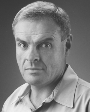 Richard K. Hester合作论文数Texas Instruments2
 Pallab K. Chatterjee合作论文数Personal Productivity Products Group, Texas Instruments, Inc.2D. W. Bellavance合作论文数2rajiv r shah合作论文数1S. S. Mahant-Shetti合作论文数1r r shah合作论文数1M. Matloubian合作论文数1Hite, L.R.合作论文数1Haken, R.A.合作论文数1
 Huatang Yuan (袁华堂)合作论文数College of Chemistry, Nankai University1C. E. C. Chen合作论文数1
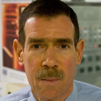 Theodore Kamins合作论文数Department of Electrical Engineering, Stanford University;Hansen Experimental Physics Laboratory, Stanford University1T. G. W. Blake合作论文数1Richard K Hester合作论文数1
 Krishna Saraswat合作论文数School of Engineering, Stanford University;Department of Electrical Engineering, Stanford University1Peng-Heng Chang合作论文数1Z. P. Sobczak合作论文数1




