Dans la perspective d'une simulation numerique de type elements-finis, les auteurs presentent la caracterisation thermomecanique d'alliages ternaires (92,5Pb-5Sn-2,5Ag et 95,5Pb-2,5Ag-2Sn) utilises dans l'industrie electronique. Au travers d'essais de flexion trois points sur DMA, la presente etude fait ressortir une forte dependance a la temperature et a la vitesse de sollicitation du module secant, de la limite d'elasticite et de la resistance a la rupture. La plage de temperatures scrutee allant de +35 a +125 °C et concernant la vitesse de sollicitation, cette derniere fut choisie entre 0,1 a 10 N.min -1 . Cette forte dependance a la temperature des trois grandeurs precitees se caracterise pour le module secant par une perte de 40 a 70 % par rapport a sa valeur initiale, de 40 a 60 % concernant la limite d'elasticite et de 40 a 45 % pour la resistance a la rupture lorque la temperature passe de +35 a +125 °C et pour une vitesse de sollicitation passant de 0,1 a 10 N.min -1 . Concernant l'influence de la vitesse de sollicitation, on observe que le module secant grimpe de 35 a 55 %, que la limite d'elasticite progresse de 20 a 50 % et que la resistance a la rupture augmente de 15 a 35 % lorsque la vitesse de sollicitation passe de 0,1 a 10 N.min -1 et pendant que la temperature passe de +35 a +125 °C.
A micromachining technique for silicon deep anisotropic etching and isolating porous silicon structures is developed. This original method combines aluminum thermomigration and silicon electrochemical etching. In this way, we have generated high aspect ratio trenches and porous silicon isolating regions as well, through the entire thickness of the wafer. In order to evaluate our method, we performed etching rate measurements varying the current density. A maximum value of 22μm∕min has been already measured. The interest of the method in terms of cost and structures diversity is also justified.
ABSTRACT We propose a new methodology for lifetime determination of PZT capacitors, based on accelerated tests performed at low voltages and high temperatures. We believe that such a methodology is the only way to characterize the relevant failure mechanism for Time-Dependent Dielectric Breakdown of PZT capacitors. The capacitors lifetime at operating conditions is found to exceed 20 years.
Since its discovery in 1956, porous silicon has found various applications according to its wide range of morphologies (chemical sensing structures, Micro-Electro-Mechanical Systems—MEMS, silicon based optoelectronics, etc.). In this paper, we present a macroporous material, with pore diameters larger than 1 μm, produced in a polarized HF/H2O mixture ([HF]=4.5 wt.%). Some square apertures were realized in a highly doped poly-silicon deposited on a thin (300 nm) silicon oxide layer. Then, electrochemical etching of the N-type 〈100〉 oriented silicon with total current densities of 5.65 and 7 mA/cm2 during 2 h were performed with a backside illumination. We observed deep trenches near the mask border, perpendicular to the surface, over 120 μm from the surface of the poly-silicon. Current density distributions have been simulated in two-dimensional structures in order to explain these phenomena.
Helium and hydrogen implantations lead to the formation of extended defects that strongly interact with impurities like metal and dopants, affecting significantly their final profiles. Even if the efficiency of this metal gettering technique is widely demonstrated in literature, the high dose requirement can be a drawback for industrial applications. Dose reduction becomes then crucial. In the smartcut (R) process, it has been shown that helium and hydrogen co-implantation leads to the expected dose decrease. The same idea was then applied for the gettering technique, keeping co-implantation doses below exfoliation threshold.After evidencing the impact of the H addition on cavities, this paper will focus on boron interactions with He-H induced defects. For this purpose, uniformly high doped (10(18) B cm(-3)) P-type < 111 > wafers were used. He implantation at 40 keV for a dose of 5 or 1 x 10(16) He+ cm(-2) followed or not by H implantation at 36 keV for different doses were carried out. Samples were subsequently furnace annealed for 1 h at temperatures ranging from 500 to 900 degrees C. Transmission electron microscopy (TEM) observations allow us to monitor the defect evolution. Secondary ion mass spectrometry (SIMS) was used to follow the boron and hydrogen profiles while the spreading resistance profiling (SRP) gives the activation dependence with the implantation and the annealing temperature. This work enlightens the large impact of H on cavity growth and clarifies the interaction of B with extended defects in presence or absence of hydrogen. (c) 2005 Elsevier B.V. All rights reserved.
High dose helium implantation followed by a suitable thermal treatment induces defects such as cavities and dislocations. Gettering efficiency of this technique for metallic impurities has been widely proved. Nevertheless, dopants, as well as point defects, interact with this defect layer. Due to the presence of vacancy type defects after helium implantation, boron diffusion can be largely influenced by such a buried layer. In this paper, we study the influence of helium induced defects on boron diffusion. The boron diffusion in presence of these defects has been analyzed as a function of different parameters such as distance between boron profile and defect layer and defect density. Our results demonstrate that the major impact known as boron enhanced diffusion can be partially or completely suppressed depending on parameters of experiments. Moreover, these results clarify the interaction of boron with extended He-induced defects.
Over the last few years, thin films of PbZrxTi1 − xO3 (PZT) have been the focus of extensive researches for high-k capacitor applications. However, we believe that the reliability properties and the degradation mechanisms of PZT capacitors need to be better understood. A good way to learn about failure mechanisms is to investigate the characteristics of leakage current conduction. In this paper we propose a model for current density evolution of IrO2/PZT/Pt structures as a function of time, voltage and temperature. The voltage and temperature evolution of leakage current is interpreted as an interface controlled thermoionic injection of carriers over a potential barrier at the cathode/PZT contact. The time evolution of the leakage current is mainly characterized by the resistance degradation phenomenon which results in a large increase in current density. A quantitative analytical model based on the redistribution of oxygen vacancies near the cathode interface has already been developed to account for this effect [1]. We propose a more complete model that also includes the role of oxygen vacancies on dielectric relaxation and trapping phenomena. The contributions of Pt and IrO2 electrodes on leakage current evolution are also discussed.
Silicon-based power device performances are largely affected by metal contamination occurring during device manufacturing. Among the usual gettering techniques, recent developments were done on high dose helium implantation. Even though the gettering efficiency of this technique has been demonstrated in device application, the required doses are still extremely high for an industrial application. Recently, it has been shown that the use of H/He co-implantation limits the total requested doses [1]. In this paper, co-implantation of H/He, which has been already used to reduce the dose in the smart-cut® process is explored. The goal of this work is to decrease efficiently the implanted dose maintaining an efficient metallic gettering without degrading the Si surface. The impact of H implantation on He implantation induced defects is carefully studied. The TEM observations have evidenced that hydrogen addition drastically modified the defect band structure and promotes the cavity growth.. Additionally, we demonstrate that an efficient gettering can be obtained.
Over the last few years, thin films of PbZx(x)Ti(1-x)O(3) (PZT) have been the focus of extensive researches for high-k capacitor applications. However, some electrical properties such as leakage current conduction and degradation mechanisms need to be better understood.From Constant Voltage Stress experiments, we identified two distinct failure mechanisms depending on the applied voltage levels. The existence of these two failure mechanisms makes it impossible to extrapolate lifetime results from high voltage to low voltage. Since the typical operating voltage for decoupling capacitors is around 3 V the reliability study has to be focused on the low voltage breakdown. A good opportunity to learn about the low voltage failure mechanisms is to investigate the characteristics of leakage current. The time evolution of leakage current is mainly controlled by the resistance degradation phenomenon. A quantitative analytical model has already been developed to account for this effect. We propose a more complete model that also includes dielectric relaxation and trapping effects. The resulting model is combined to a charge-influenced thermoionic emission model that fits fairly well the voltage and temperature dependence of leakage current. The static and dynamic parts of our model are found to be consistent, especially in terms of barrier lowering effect induced by the resistance degradation process. We believe that the low voltage breakdown is related to a trapping-induced creation of defects in the film. (c) 2005 Elsevier B.V. All rights reserved.
Wafer level reliability is a key tool for the development of new technologies, since it enables to anticipate the lifetime of these technologies in operating conditions. In this paper, we present a testing methodology for lifetime extrapolation of high density PZT capacitors. This study is related to a basic time-dependent dielectric breakdown characterization, from which we could identify several failure mechanisms, depending on the applied voltage stress level. The proposed testing methodology, based on cumulated voltage and temperature accelerations, enables to emulate only the relevant failure mechanism for lifetime extrapolation. Assuming an E model for voltage extrapolation and a top electrode perimeter scaling for geometry dependency, we finally developed a complete reliability model that takes into account the temperature, voltage and geometry influences on capacitors lifetime.
Reliability tests and simulated results on medium power components are discussed in this paper. This study is based on statistical data coming from thermal cycling tests (TCT, air-air test) and thermal shock tests (TST, liquid-liquid test), which are correlated with information coming from failure analysis and compared to results issued from 3D finite element (FE) analysis.
Deep single trenches can be produced at the edge of apertures of protective films masking the surface of silicon samples. This macropore formation, from polarized HF based solutions, is electrically activated depending on the mask geometrical and physical parameters whatever the silicon type or the electrolyte composition. The mask thickness increase is known to induce deeper trenches. In this paper, we show that we can predict and localize this phenomenon by simulating two dimensional hole current distributions below the mask. We demonstrate also the influence of the material permittivity on trench depth. These 2D simulation results are correlated with experimental results.
This paper presents different contact test structures intended to characterize the metal–semiconductor interface (aluminum–silicon) for power integrated circuits fabricated in the Application Specific Discrete (ASD™) process technologies. For this study, three contact test structures have been selected, transfer length method (TLM), cross bridge Kelvin resistance (CBKR), and contact end resistance (CER). The characterization is achieved by extracting the specific contact resistance (ρC) from contact test structures by measuring the contact resistance (RC). To validate the results, spreading resistance was used to determine the surface doping concentration (CS) of the diffused layer that gives ρC from a well know standard abacus. From the experimental results, we conclude that only the TLM test structure is able to give correct values of the specific contact resistance for both n and p type diffused layers that are compatibles with the manufacturer specifications.
Magnesium oxide (MgO) thin films have been studied as an alternative dielectric to silicon dioxide (SiO2) for SiC insulation applications. Thin MgO films have been deposited onto Pt/Si substrate, using sol-gel coating process. Theta-2theta X-ray diffraction patterns of the films show a [I I I] preferential orientation. MIM structures have been elaborated to characterize the electrical properties of the sol-gel MgO films. Current-Voltage characteristics of these structures have been measured between 150degreesC and 250degreesC. The first IN curves show two conduction regimes: an ohmic-like regime at low electrical fields (E<0.3MV/cm), and a Schottky-type regime at higher electrical fields (E>0.3MV/cm). Zero-field potential barrier heights of the order of I eV have been estimated.
In this work, the first reliability results of Thermal Cycling Tests (TCT, air-air test) and Thermal Shock Tests (TST, liquid-liquid test) on medium power electronic components are discussed. The influence of dwell times, extremes temperatures and mean temperature is investigated. This study is based on statistical data correlated with information coming from failure analysis and confirmed by a basic FEM analysis. (C) 2004 Elsevier Ltd. All rights reserved.
High dose helium implantation leads to the formation of extended defects, such as cavities and dislocations that interact with impurities like metals and dopants, affecting their final profiles. The detailed mechanisms governing the boron segregation on these defects are still unclear. In this paper, we evidence that the boron diffusivity is decreased when boron is implanted between the surface and the He-induced defect layer. This layer acts as a sink for interstitials. Using “flat profile” experiments, we propose a simple trapping model of boron at the He-induced extended defects. Numerical modeling has been performed to extract the boron effective diffusion coefficient with regard to the defect band. This work emphasizes the impact of effective diffusivity variation on the boron gettering phenomenon and clarifies boron interaction with He-induced defects.
Silicon carbide (SiC) is a wide bandgap semiconductor suitable for high-voltage, high-power, and high-temperature devices from DC to microwave frequencies. However, the marketing of advanced SiC power devices remains limited due to performance limitation of the SiO2 dielectric among other issues. Indeed, SiO2 has a dielectric constant 2.5 times lower than SiC, which means that at critical field for breakdown in SiC, the electric field in the adjoining SiO2 becomes too high for reliable operation. This suppresses the main advantage of using SiC power devices if the ten times higher breakdown field for SiC in comparison to Si cannot be exploited. Therefore, alternative dielectrics having a dielectric constant higher or in the same order as SiC (εr≈10) should be used to reduce the electrical field in the insulator. Among alternative dielectrics to silicon dioxide (SiO2), magnesium oxide (MgO) seems to be a good candidate regarding its bulk properties: large bandgap, high thermal conductivity and stability, and a suitable dielectric constant (εr≈10). In order to evaluate such a promising candidate, the sol–gel process appears to be a convenient route to elaborate this kind of coatings. By selecting an appropriate precursor solution and optimizing the curing conditions of the films, MgO films could be obtained under various crystallization states: non-oriented or preferred [111] orientation. MIM structures have been used to investigate the insulating properties of the sol–gel MgO films. The dielectric strength of the films was found to be microstructure–dependent, and reached 3 to 8MV/cm at room temperature. Leakage currents were measured from 150 up to 250°C, with values less than 10−5A/cm2 at 1MV/cm.
Processing issues for the fabrication of capacitive micromachined ultrasonic transducer (cMUT) arrays have been studied using surface micromachining. This work focuses on the critical steps of process fabrication such as membrane formation, sacrificial layer properties and vacuum sealing performance of cavity. We describe a four-mask process for the realization of sealed cMUT. We demonstrate that the use of a sacrificial layer with a columnar structure gives a fast etching rate (29 nm s−1) in a buffered hydrofluoric acid solution. The mechanical stress of LPCVD silicon nitride (SiNx), used as membrane, was evaluated. We compared the vacuum sealing performance of different materials in order to find the best material in terms of lateral deposition inside the cavity. Functional transducers have been obtained. We proposed an electrical test in order to evaluate the vacuum sealing of the cavity based on the collapse voltage determination. Laser interference measurements were used to characterize the dynamic displacement of the membrane.
The authors explain the degradation mechanism of a TRIAC submitted to the application of strong di/dt during the turn-on in quadrant Q3. From reliability results, analysis of the failure modes and thermo-mechanical simulation of the structure, the authors propose a degradation model, which can be used to give the number of commutation cycles before failure of the component.
 Jean Oualid合作论文数18
 Daniel Alquier合作论文数STMicroelectronics SA, STMicroelectronics12Laurent Ventura合作论文数9
 Thierry Lequeu合作论文数LMP-STMicroelectronics8F. Cayrel合作论文数8Charles Dubois合作论文数7Etienne Ciantar合作论文数7
 Jean-Michel Moragues合作论文数7
 Daniel Mathiot合作论文数6
 F. Roqueta合作论文数6Stéphane Moreau合作论文数5J. P. Loup合作论文数5Bruno Sagnes合作论文数5
 Guillaume Guegan合作论文数4S. Forster合作论文数4
 Slimane Oussalah合作论文数4J. Dugas合作论文数4
 Emilien Bouyssou合作论文数4G. Gaudin合作论文数3ch ortiz合作论文数3
 Sorin Cristoloveanu合作论文数3
 Gaël Gautier合作论文数Université François Rabelais de Tours, Laboratoire de Microélectronique de Puissance, 16 Rue Pierre et Marie Curie, BP 7155, 37071 Tours Cedex 2, France3J.M. Mirabel合作论文数3k yckache合作论文数2F. Guillet合作论文数2ch dubois合作论文数2
 Leo Vincent合作论文数2P. Prené合作论文数2Seghir, H.合作论文数2
 Philippe Leduc合作论文数2J.J. Grob合作论文数2
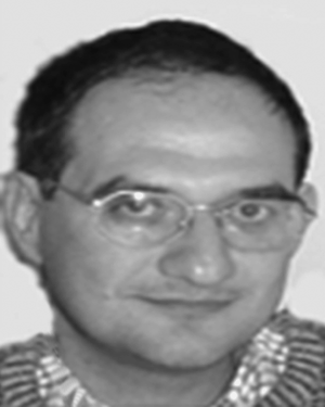 Vito Raineri合作论文数2C. Anceau合作论文数2
 Corrado Bongiorno合作论文数Consiglio Nazionale delle Ricerche - Istituto per la Microelettronica e Microsistemi2D. Labrunye合作论文数2Céline Bondoux合作论文数2S. Burgniard合作论文数2
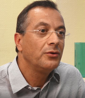 Philippe Belleville合作论文数CEA2
 Dominique Vuillaume合作论文数Centre National De La Recherche Scientifique2René Leroy合作论文数1C. Leborgne合作论文数1Y. Mentalecheta合作论文数1M. Roy合作论文数1J Baborowski合作论文数1
 Stéphane Lefebvre合作论文数1Belgacem, B.合作论文数1
 L. Dupont合作论文数Laboratoire de Réactivité et de Chimie des Solides, Univerisity of Picardie Jules Verne1
 Paul Muralt合作论文数Ecole Polytechnique Federale de Lausanne1S. Martinuzzi合作论文数1




