We present a method for assessing the quality of electronic material properties of thin-film metal-oxide-semiconductor field-effect transistors (MOSFETs). By investigating samples with metal-organic-chemical-vapor-deposition (MOCVD)-grown molybdenum disulfide (MoS2) channels exposed to atmospheric conditions, we reveal the existence of electron traps in MoS2 and at the interface between the gate insulator and the thin-film MoS2. Differential conductance and capacitance data of the transistor channels are plotted as 3-D surfaces on a base plane spanned by the measurement frequency versus the gate voltage. The existence of defects is confirmed by comparison with ideal results from a theoretical model.
The transition regions of GdSiO/SiOx and HfO2/SiOx interfaces have been studied with the high-k layers deposited on silicon substrates. The existence of transition regions was verified by medium energy ion scattering (MEIS) data and transmission electron microscopy (TEM). From measurements of thermally stimulated current (TSC), electron states were found in the transition region of the HfO2/SiOx structures, exhibiting instability attributed to the flexible structural molecular network expected to surround the trap volumes. The investigations were focused especially on whether the trap states belong to an agglomeration consisting of a single charge polarity or of a dipole constellation. We found that flat-band voltage shifts of MOS structures, that reach constant values for increasing oxide thickness, cannot be taken as unique evidence for the existence of dipole layers.
Starting from a quantum statistical reasoning, it is demonstrated that entropy properties of silicon/silicon dioxide interface electron traps may have a strong influence on measured distributions of interface states, depending on measurement method used. For methods, where the Fermi-level is used as a probe to define an energy position, the scale is based on free energy. On the other hand, methods based on thermal activation of electrons give the distribution on an enthalpy scale. It is shown that measured interface state distributions are influenced by the distribution of entropy, and that common features of measured energy distributions may be influenced by entropy variations. These results are used to interpret experimental data on the energy distribution of electron capture cross sections with an exponential increase followed by a more or less constant value as the energy distance of the traps from the conduction band edge increases. Such a relation is shown to be consistent with a situation where the emission and capture processes of electrons obey the Meyer-Neldel rule.
We use Multi Parameter Admittance Spectroscopy (MPAS) for characterizing trapped charge in molybdenum disulphide (MoS 2 ) based field-effect transistors (FETs). The method relies on frequency and voltage dependent admittance measurements and aims at characterization of energy positions and carrier emission rate of the traps. This characterization gives information about trap distributions in the MoS 2 and the influence of traps in the gate oxide bulk.
Heterostructures comprising silicon, molybdenum disulfide (MoS2), and graphene are investigated with respect to the vertical current conduction mechanism. The measured current-voltage (I-V) characteristics exhibit temperature-dependent asymmetric current, indicating thermally activated charge carrier transport. The data are compared and fitted to a current transport model that confirms thermionic emission as the responsible transport mechanism across devices. Theoretical calculations in combination with the experimental data suggest that the heterojunction barrier from Si to MoS2 is linearly temperature-dependent for T = 200-300 K with a positive temperature coefficient. The temperature dependence may be attributed to a change in band gap difference between Si and MoS2, strain at the Si/MoS2 interface, or different electron effective masses in Si and MoS2, leading to a possible entropy change stemming from variation in density of states as electrons move from Si to MoS2. The low barrier formed between Si and MoS2 and the resultant thermionic emission demonstrated here make the present devices potential candidates as the emitter diode of graphene base hot electron transistors for future high-speed electronics.
Molybdenum disulfide (MoS 2 ) is a semiconducting transition metal dichalcogenide material. This two-dimensional (2D) layered material has a band gap ranging from 1.3 eV in bulk form (indirect) to 1.88 eV as a monolayer (direct). The material has been suggested as a potential candidate for applications in nanoelectronics, optoelectronics and neuromorphic computing [1]–[4]. In this talk, the principles of scalable growth through thermal conversion of metals and metal-organic vapor phase growth will be discussed [5], [6]. These materials are then integrated into the silicon technology platform to demonstrate device applications. Conventional field effect transistors with MoS 2 channels show promising characteristics. In addition, ion-based plasticity promises to enable memristive functionality on MoS 2 devices. In particular, vertically aligned MoS 2 layers allow the tuning of energy barriers at MoS 2 /semiconductor Schottky junctions through mobile ions [7], [8]. These ions (OH - ) likely originate from catalytic splitting of water molecules. Spectral response measurements of MoS 2 based devices provide insight into the band structure and beyond, as photodetectors based on MoS 2 /silicon/graphene and MoS 2 /amorphous silicon heterostructures show peculiar responsivity in the infrared regime [9]–[11]. Acknowledgements The authors acknowledge funding through the European Union’s Horizon 2020 research and innovation programme under grant agreements 785219 (Graphene Flagship) and 829035 (QUEFORMAL), the German BMBF grant NEUROTEC (16ES1134) and the DFG projects MOSTFLEX (407080863) and ULTIMOS 2 (412113712). References [1] K. F. Mak, C. Lee, J. Hone, J. Shan, and T. F. Heinz, “Atomically Thin MoS 2 : A New Direct-Gap Semiconductor,” Phys. Rev. Lett. , vol. 105, no. 13, p. 136805, Sep. 2010. [2] B. Radisavljevic and A. Kis, “Mobility engineering and a metal–insulator transition in monolayer MoS2,” Nat. Mater. , vol. 12, no. 9, pp. 815–820, Sep. 2013. [3] A. Bablich, S. Kataria, and M. C. Lemme, “Graphene and Two-Dimensional Materials for Optoelectronic Applications,” Electronics , vol. 5, no. 1, p. 13, Mar. 2016. [4] V. K. Sangwan et al. , “Multi-terminal memtransistors from polycrystalline monolayer molybdenum disulfide,” Nature , vol. 554, no. 7693, pp. 500–504, Feb. 2018. [5] S. Kataria et al. , “Growth-Induced Strain in Chemical Vapor Deposited Monolayer MoS 2 : Experimental and Theoretical Investigation,” Adv. Mater. Interfaces , vol. 4, no. 17, p. 1700031, Sep. 2017. [6] M. Marx et al. , “Large-area MoS 2 deposition via MOVPE,” J. Cryst. Growth , vol. 464, pp. 100–104, Apr. 2017. [7] M. Belete et al. , “Dielectric Properties and Ion Transport in Layered MoS 2 Grown by Vapor-Phase Sulfurization for Potential Applications in Nanoelectronics,” ACS Appl. Nano Mater. , vol. 1, no. 11, pp. 6197–6204, Nov. 2018. [8] M. Belete et al. , “Nonvolatile Resistive Switching in Nanocrystalline Molybdenum Disulfide with Ion-Based Plasticity,” arXiv:1911.06032 , 2019. [9] C. Yim et al. , “Heterojunction Hybrid Devices from Vapor Phase Grown MoS 2 ,” Sci. Rep. , vol. 4, Jun. 2014. [10] M. Belete et al. , “Large Scale MoS 2 /Si Photodiodes with Graphene Transparent Electrodes,” presented at the European Solid-State Device Research Conference (ESSDERC), Krakow, Poland, 2019. [11] A. Bablich et al. , “Few-Layer MoS 2 /a-Si:H Heterojunction Pin-Photodiodes for Extended Infrared Detection,” ACS Photonics , vol. 6, no. 6, pp. 1372–1378, Jun. 2019.
Non‐volatile resistive switching is demonstrated in memristors with nanocrystalline molybdenum disulfide (MoS 2 ) as the active material. The vertical heterostructures consist of silicon (Si), vertically aligned MoS 2 , and chrome/gold metal electrodes. Electrical characterizations reveal a bipolar and forming‐free switching process with stable retention for at least 2500 s. Controlled experiments carried out in ambient and vacuum conditions suggest that the observed resistive switching is based on hydroxyl ions (OH − ). These originate from catalytic splitting of adsorbed water molecules by MoS 2 . Experimental results in combination with analytical simulations further suggest that electric field driven movement of the mobile OH − ions along the vertical MoS 2 layers influences the energy barrier at the Si/MoS 2 interface. The scalable and semiconductor production compatible device fabrication process used in this work offers the opportunity to integrate such memristors into existing Si technology for future neuromorphic applications. The observed ion‐based plasticity may be exploited in ionic‐electronic devices based on transition metal dichalcogenides and other 2D materials for memristive applications.
Heterostructures of two-dimensional (2D) and three-dimensional (3D) materials form efficient devices for utilizing the properties of both classes of materials. Graphene/silicon (G/Si) Schottky diodes have been studied extensively with respect to their optoelectronic properties. Here, we introduce a method to analyze measured capacitance-voltage data of G/Si Schottky diodes connected in parallel with G/silicon dioxide/Si (GIS) capacitors. We also demonstrate the accurate extraction of the built-in potential ($\Phi$$_{bi}$) and the Schottky barrier height from the measurement data independent of the Richardson constant.
Photodiodes comprising n(+)-silicon / molybdenum disulfide (MoS2) / graphene heterojunctions configured in a vertical architecture are investigated. The silicon substrates have been fabricated in a silicon pilot line using standard silicon process technology. The two-dimensional MoS2 has been grown from thin, pre -patterned molybdenum films in a sulfur environment through thermally assisted conversion (TAC). Graphene has been grown through chemical vapor deposition and transferred onto the MoS2 / Si diodes as a transparent conductor. Under reverse DC-bias, the heterojunction photodiodes exhibit a spectral responsivity that is a fingerprint of the combined materials and their direct and indirect band transitions. In addition, the diodes show finite responsivity in the infrared, below the band gaps of MoS2 and Si, which is attributed to the broadband absorption in the graphene electrodes and/or defect states in the MoS2. The work demonstrates the feasibility of scalable integration of two-dimensional materials with conventional silicon processes technology, and provide a substantial contribution towards the realization of scalable next generation optoelectronic devices based on 2D materials.
Graphene/silicon (G/Si) heterostructures have been studied extensively in the past years for applications such as photodiodes, photodetectors, and solar cells, with a growing focus on efficiency and performance. Here, a specific contact pattern scheme with interdigitated Schottky and graphene/insulator/silicon (GIS) structures is explored to experimentally demonstrate highly sensitive G/Si photodiodes. With the proposed design, an external quantum efficiency (EQE) of >80% is achieved for wavelengths ranging from 380 to 930 nm. A maximum EQE of 98% is observed at 850 nm, where the responsivity peaks to 635 mA/W, surpassing that of conventional Si p-n photodiodes. This efficiency is attributed to the highly effective collection of charge carriers photogenerated in Si under the GIS parts of the diodes. The experimental data is supported by numerical simulations of the diodes. On the basis of these results, a definition for the “true” active area in G/Si photodiodes is proposed, which may serve toward standardization of G/Si-based optoelectronic devices.
Few-layer molybdenum disulfide (FL-MoS2) films have been integrated into amorphous silicon (a-Si:H) pin-photodetectors. To achieve this, vertical a-Si:H photodiodes were grown by plasma-enhanced chemical vapor deposition (PE-CVD) on top of large-scale synthesized and transferred homogeneous FL-MoS2. This novel detector array exhibits long-term stability (more than six month) and outperforms conventional silicon-based pin-photodetectors in the infrared range (IR, λ = 2120 nm) in terms of sensitivities by up to ∼50 mAW–1. Photodetectivities of up to ∼2 × 10¹⁰ Jones and external quantum efficiencies of ∼3% are achieved. The detectors further feature the additional functionality of bias-dependent responsivity switching between the different spectral ranges. The realization of such scalable detector arrays is an essential step toward pixelated and wavelength-selective sensors operating in the IR spectral range.
Electronic and dielectric properties of vapor-phase grown MoS2 have been investigated in metal/MoS2/silicon capacitor structures by capacitance-voltage and conductance-voltage techniques. Analytical methods confirm the MoS2 layered structure, the presence of interfacial silicon oxide (SiO x ) and the composition of the films. Electrical characteristics in combination with theoretical considerations quantify the concentration of electron states at the interface between Si and a 2.5-3 nm thick silicon oxide interlayer between Si and MoS2. Measurements under electric field stress indicate the existence of mobile ions in MoS2 that interact with interface states. On the basis of time-of-flight secondary ion mass spectrometry, we propose OH- ions as probable candidates responsible for the observations. The dielectric constant of the vapor-phase grown MoS2 extracted from CV measurements at 100 kHz is 2.6 to 2.9. The present study advances the understanding of defects and interface states in MoS2. It also indicates opportunities for ion-based plasticity in 2D material devices for neuromorphic computing applications.
Graphene has great potential in flexible and rigid optoelectronic devices due to its atomic thickness (and hence flexibility), high conductivity and broadband transparency [1], [2]. Graphene forms a Schottky junction with semiconductor materials, which can be exploited as simple photodiodes [3], [4]. Recently, it was reported that insulated regions in graphene/silicon (G/Si) photodiodes, e.g. regions separated by oxides to allow contacting the graphene, have a significant contribution towards the extracted photocurrent [5], [6]. Based on these findings, we have optimized the design of graphene-based photodiodes. Here, we report on these graphene/silicon Schottky diodes with very high responsivity, including analysis of the spectral “fingerprint”. Scanning photocurrent measurements (SPCM) support our claims as they provide local spatial distributions of photocurrents in the devices. Based on our experiments, we revisit the extraction of responsivity in previous literature, where the insulating regions have been largely ignored when calculating it. This leads to a distinct overestimation of responsivity.
Graphene/silicon (G/Si) heterojunction based devices have been demonstrated as high responsivity photodetectors that are potentially compatible with semiconductor technology. Such G/Si Schottky junction diodes are typically in parallel with gated G/silicon dioxide (SiO2)/Si areas, where the graphene is contacted. Here, we utilize scanning photocurrent measurements to investigate the spatial distribution and explain the physical origin of photocurrent generation in these devices. We observe distinctly higher photocurrents underneath the isolating region of graphene on SiO2 adjacent to the Schottky junction of G/Si. A certain threshold voltage (VT) is required before this can be observed, and its origins are similar to that of the threshold voltage in metal oxide semiconductor field effect transistors. A physical model serves to explain the large photocurrents underneath SiO2 by the formation of an inversion layer in Si. Our findings contribute to a basic understanding of graphene/semiconductor hybrid devices which, in turn, can help in designing efficient optoelectronic devices and systems based on such 2D/3D heterojunctions.
A semiempirical model describing the influence of interface states on characteristics of gate capacitance and drain resistance versus gate voltage of top gated graphene field effect transistors is presented. By fitting our model to measurements of capacitance–voltage characteristics and relating the applied gate voltage to the Fermi level position, the interface state density is found. Knowing the interface state density allows us to fit our model to measured drain resistance–gate voltage characteristics. The extracted values of mobility and residual charge carrier concentration are compared with corresponding results from a commonly accepted model which neglects the effect of interface states. The authors show that mobility and residual charge carrier concentration differ significantly, if interface states are neglected. Furthermore, our approach allows us to investigate in detail how uncertainties in material parameters like the Fermi velocity and contact resistance influence the extracted values of interface state density, mobility, and residual charge carrier concentration.
The use of graphene as a material for metal-oxide-graphene field-effect transistors (MOGFETs) is a possible overture to an epoch of faster electronics with properties similar to the traditional MOSFET, yet including interesting novel restrictions and possibilities [1]. This is apparent for the gate capacitor, where a two-dimensional graphene layer, constituting the transistor channel, is in intimate contact with a high-k oxide under a gate metal. Thermal activation of trapped charge carriers from interface states and border traps into the energy bands is a common feature of oxide-semiconductor systems. In contrast, due to the lack of an energy bandgap in monolayer graphene, the transfer of charge carriers in oxide traps into states of the channel material takes place as tunneling processes, serving the electron and hole exchange. In the paper, a background is given for modelling capacitance versus voltage data for MOG capacitors and transfer characteristics for MOGFETs. The derivation is founded on the position of the Fermi-level in the graphene layer, which determines all dynamic charge in the system at thermal equilibrium. In the first step, C-V and transfer characteristics for structures with oxides, comprising single electron trap states, will be given. This includes the dependence on temperature and on the frequency used for the probing signal of the capacitance meter. For high-k oxides, the dominating trap constellations consist of oxygen vacancies with varying atomic geometries, depending on the number of occupying carriers. Capturing charge carriers into electron and hole states in the core of the trap volume, the bonds between the surrounding atoms may change character. Accordingly, when an electron is captured into such traps, the (free) energy exchange in the transfer sequence not merely includes electron energy, but also the change in lattice energy needed for the process. Besides the energy carried by the charge carrier from the “sheet of electrons” in the graphene, also mechanical energy is required to change the atomic part of the trap assembly. This latter quantity is supplied by local phonons within the trap volume [2]. Converting the atomic arrangement when turning from one electronic state to another thus includes local vibrational energy, which requires thermal activation for the atomic transition. Therefore, the emission and capture rates for transitions between the oxide traps and the graphene are limited by a combination of the tunneling between electron states and the change in atomic arrangement. An example for a single electron trap is shown in Fig. 1, depicting the electron tunneling transition from graphene into the electron state E 1 for a trap able to capture one electron. Simultaneously, this requires a transition of the atomic vibrational states from Osc. 0 to Osc. 1, which includes thermal activation to the crossing point between these energy potentials, and thus an atomic energy exchange of U 0as noted in the figure. The discussion will be further extended to multiple electron traps, where we find that thermal activation occurs as a stepping process between atomic potentials, depending on internal vibrational excitations of the atoms surrounding the electronic trap state. It will be demonstrated that the emission and capture rates of charge carriers may depend on the ramping direction of the gate voltage in a measurement cycle, which gives rise to specific hysteresis effects for traps with atomic relaxation properties. Finally, single traps positioned close to the graphene layer may create electrical potential variations (“puddles”) along the channel [3]. This will locally change the position of the Fermi-level in the graphene, generate a varying energy position of the graphene Dirac-point and influence the shape of C-V and transfer curves. References [1] M.C. Lemme et al., MRS Bulletin, 39(8), 711-718 (2014) [2] O. Engström, ”The MOS System”, (Cambridge University Press, 2014); ECS Transactions, 35 (4), 19 -38 (2011) [3] J. Martin et al., Nat. Phys., 4, 144-148 (2008) Figure 1
For each new generation in MOS-technology, a recurrent problem has been the so-called “short channel effect.” It occurs when decreasing the gate length such that the edge of the depletion region at drain approaches the source contact close enough for increasing the leakage between source and drain and for decreasing the transistor threshold voltage (Fig. 11.1(a)). For bulk CMOS technology, the standard method to avoid this issue has been to increase the doping in the channel region in order to decrease the depletion region width of the drain junction. This measure, however, decreases the capacitive coupling between gate and channel and lowers the share of the gate voltage falling across the semiconductor channel. As a consequence, the sub-threshold slope decreases, which in turn slows down the switching speed of the transistor. Furthermore, increased doping levels in the channel give rise to higher scattering probabilities and lowered charge carrier mobility. These problems can be avoided by decreasing the thickness of the gate oxide in order to increase the capacitance between gate and channel such that the oxide capacitance becomes much larger than the channel capacitance and gives a major share of the applied gate voltage to the semiconductor. Measures along these lines were possible until the gate length downscaling reached about 45 nm. At this landmark, the SiO2 dielectric needed to reach a thickness of about 1.5 nm, which gave rise to unacceptable gate leakage levels (Taur et al., 1998; Iwai and Ohmi, 2002; Iwai, 2009; Wong and Iwai, 2006; Frank, 2011).
 M. Kaniewska合作论文数Institute of Electron Technology, Department of Analysis of Semiconductor Nanostructures, Al. Lotników 32/46, 02-668 Warsaw, Poland32
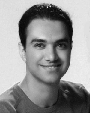 Bahman Raeissi合作论文数31
 Max Lemme合作论文数Faculty of Electrical Engineering and Information Technology, RWTH Aachen University;AMO GmbH30
 Paul K. Hurley合作论文数NMRC, University College Cork22J. Piscator合作论文数22
 Karim Cherkaoui合作论文数Tyndall National Institute, University College Cork20H. D. B. Gottlob合作论文数19
 Stephen Hall合作论文数University of Liverpool18Stefan Bengtsson合作论文数17Mariusz Kaczmarczyk合作论文数17
 Mats Andersson合作论文数Flinders Institute for Nanoscale Science and Technolog, Flinders University;College of Science and Engineering, Flinders University;Chalmers University of Technology12
 Ivona Mitrovic合作论文数Department of Electrical Engineering and Electronics, University of Liverpool;School of Electrical Engineering, Electronics and Computer Science, Faculty of Science and Engineering, University of Liverpool12
 Einar O. Sveinbjornsson合作论文数Inst Sci, Univ Iceland11
 Satender Kataria合作论文数10Jauhiainen, Anders合作论文数9
 Octavian Buiu合作论文数Department of Electrical Engineering and Electronics, University of Liverpool9G. Zaremba合作论文数8Kenneth R. Farmer合作论文数8
 Joao Marcelo Jordao Lopes合作论文数Department of Epitaxy, Paul Drude Institute for Solid State Electronics8Gi Andersson合作论文数7M. Schmidt合作论文数7Ying Fu合作论文数7
 Johan Piscator合作论文数7
 Melkamu Belete合作论文数Chair of Electronic Devices, RWTH Aachen University6SB Newcomb合作论文数6J. Schubert合作论文数6
 Scott Monaghan合作论文数Tyndall National Institute, University College Cork6
 Wojciech Jung合作论文数5Henryk M. Przewlocki合作论文数5Anke Sanz-Velasco合作论文数5B. Liss合作论文数4
 Sarah Riazimehr合作论文数4
 H. Kurz合作论文数4
 Alim Karmous合作论文数4
 Paul Chalker合作论文数School of Engineering, University of Liverpool4Barbara Surma合作论文数4Tomasz Gutt合作论文数3
 Eros Reato合作论文数Chair of Electronic Devices, RWTH Aachen University3f ducroquet合作论文数3
 Omid Habibpour合作论文数Dept. of Microtechnol. &Nanosci., Chalmers Univ. of Technol.;c;Dept. of Microtechnol. & Nanosci., Chalmers Univ. of Technol.3
 Daniel S. Schneider合作论文数3
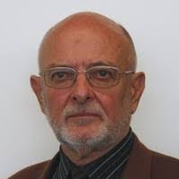 Erich Kasper合作论文数Department of Electrical Engineering and Information Technology, University of Stuttgart3W. Davey合作论文数3
 Mohammadsadegh Sadeghi合作论文数3
 A. Godoy合作论文数Departamento de Electrónica y Tecnología de Computadores, Universidad de Granada3
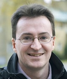 Per Lundgren合作论文数Department of Clinical Sciences, Norrlands University Hospital3
 Jan Stake合作论文数Microwave Electronics Laboratory;Chalmers University of Technology;Microwave Electronics Laboratory, Chalmers University of Technology3
 Zhenxing Wang (王振兴)合作论文数National Center for Nanoscience and Technology, Chinese Academy of Sciences3M. Pacholak-Cybulska合作论文数3




