Recent CAD methodologies of design-for-manufacturability (DFM) have naturally led to a significant increase in the number of process and layout parameters that have to be taken into account in design-rule checking. Methodological consistency requires that a similar number of parameters be taken into account during layout parasitic extraction. Because of the inherent variability of these parameters, the issue of efficiently extracting deterministic parasitic sensitivities with respect to such a large number of parameters must be addressed. In this paper, we tackle this very issue in the context of capacitance sensitivity extraction. In particular, we show how the adjoint sensitivity method can be efficiently integrated within a finite-difference (FD) scheme to compute the sensitivity of the capacitance with respect to a large set of BEOL parameters. If np is the number of parameters, the speedup of the adjoint method is shown to be a factor of np/2 with respect to direct FD sensitivity techniques. The proposed method has been implemented and verified on a 65 nm BEOL cross section having 10 metal layers and a total number of 59 parameters. Because of its speed, the method can be advantageously used to prune out of the CAD flow those BEOL parameters that yield a capacitance sensitivity less than a given threshold.
Full package signal integrity analysis is parallelized in a suite of tools called PATS (package analysis tool suite). PATS extracts sparse circuit models using a segment-to-segment BEM (boundary element method) algorithm for both capacitance and inverse inductance and uses a fixed-time step circuit simulator to create time-domain scattering models. Critical issues regarding the parallelization of PATS and segment-to-segment BEM circuit models are explored. Examples demonstrating the accuracy of this approach are presented for real packaging cases
We present a noise-driven effective capacitance method for estimating the combined propagation noise and crosstalk noise. Gate propagation noise rules are efficiently calculated inside the Ceff procedure to determine a linear Thevenin model of the victim driver. A voltage-dependent current source model (Croix and Wong, 2003 and Keller et al.,2004) of the driver, along with a load capacitor is analyzed to generate the gate output waveform, from which noise rules are directly extracted. This method removes potential errors introduced in traditional look-up table or fitted-equation based noise rules. The linear driver Thevenin model can then be employed to analyze the propagation noise, while the same Thevenin resistance can be used to analyze the crosstalk noise. The combined coupling and propagation noise can then be estimated using superposition. In this work, we extend the popular timing-driven effective capacitance method into the noise domain. Similar to the effective capacitance method in timing analysis, this technique can successfully separate the nonlinear driver analysis from the linear interconnect analysis. In addition, the linear driver model can significantly ease the task of finding the worst-case peak alignment among all the victim and aggressor noise sources. Experimental results on both RC and RLC nets from industry designs show both accuracy and efficiency compared to SPICE results.
One means of reducing pessimism in crosstalk analysis is to consider timing orthogonality. While earlier works have addressed the temporal alignment of timing windows [1, 2, 3, 4], these treatments have overlooked one key point. Crosstalk noise failures are frequency dependent. A chip that functions at one frequency can fail due to crosstalk noise at faster and slower frequencies. Moreover, because system developers and manufacturers need chips that operate over a wide range of frequencies, noise analysis tools should guarantee a wide range of operation. In this paper, we explain this phenomenon and propose a simple procedure to include timing information and guarantee functionality from dc to f(max).
Although three-dimensional (3-D) partial inductance modeling costs have decreased with stable, sparse approximations of the inductance matrix and its inverse, 3-D models are still intractable when applied to full chip timing or crosstalk analysis. The 3-D partial inductance matrix (or its inverse) is too large to be extracted or simulated when power-grid cross-sections are made wide to capture proximity effect and wires are discretized finely to capture skin effect. Fortunately, 3-D inductance models are unnecessary in VLSI interconnect analysis. Because return currents follow interconnect wires, long interconnect wires can be accurately modeled as two-dimensional (2-D) transmission lines and frequency-dependent loop impedances extracted using 2-D methods . Furthermore, this frequency dependence can be approximated with compact circuit models for both uncoupled and coupled lines. Three-dimensional inductance models are only necessary to handle worst case effects such as simultaneous switching in the end regions. This paper begins by explaining and defending the 2-D modeling approach. It then extends the extraction algorithm to efficiently include distant return paths. Finally, a novel synthesis technique is described that approximates the frequency-dependent series impedance of VLSI interconnects with compact circuit models suitable for timing and noise analysis.
A coupling noise evaluation of a high performance S/390 microprocessor using a full chip RLC extraction and simulation process is presented. Review of on-chip wiring guidelines with respect to the inaccuracies of an RC coupling evaluation for known net topologies is discussed in terms of tool requirements for full-chip noise evaluation which include inductive coupling effects. The extraction and simulation approach is described in terms of algorithms and procedures used to account for the frequency dependent RLC effects in a manner that allow a full chip noise evaluation. Results are presented which compare noise amplitude differences between RC and R(f)L(f)C evaluations for the wiring data of an S/390 microprocessor as well as pertinent statistics such as run times and memory usage
A coupling noise evaluation of a high performance S/390 microprocessor using a full chip RLC extraction and simulation process is presented. Review of on-chip wiring guidelines with respect to the inaccuracies of an RC coupling evaluation for known net topologies is discussed in terms of tool requirements for full-chip noise evaluation which include inductive coupling effects. The extraction and simulation approach is described in terms of algorithms and procedures used to account for the frequency dependent RLC effects in a manner that allow a full chip noise evaluation. Results are presented which compare noise amplitude differences between RC and R(f)L(f)C evaluations for the wiring data of a S/390 microprocessor as well as pertinent statistics such as run times and memory usage.
A GaAs, enhanced/depletion mode, self-aligned, refractory-gate, MESFET chip process and circuit family have been developed for the integration of fiber-optic data link functions (e.g. photodetection, amplification, clock recovery, and deserialization) on a single chip. These authors describe the process and present results on integrating a complete optical receiver, including the photodiode and cl...
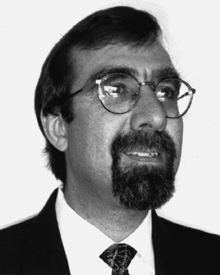 Byron Krauter合作论文数9
 Gerard V. Kopcsay合作论文数5
 Alina Deutsch合作论文数IBM T. J. Watson Research Center5
 Ibrahim Elfadel合作论文数Masdar Institute, Khalifa University;Center for Cyber-Physical Systems, Khalifa University;Laboos Technologies4lewis william dewey合作论文数3Howard H Smith合作论文数3
 Sharad Mehrotra合作论文数Donald Bren School of Information and Computer Sciences, University of California, Irvine3
 Chandramouli V. Kashyap合作论文数3m a bowen合作论文数2gregory schaeffer合作论文数2
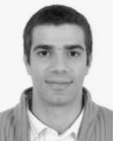 Tarek A. El-Moselhy合作论文数Massachusetts Institute of Technology2Barry J. Rubin合作论文数2Allan H. Dansky合作论文数2Tarek El-Moselhy合作论文数1S. Bermon合作论文数1EP HARRIS合作论文数1parsotam t patel合作论文数1B. J. Rubin合作论文数1Jd Crow合作论文数1peter d hoh合作论文数1Patrick M. Williams合作论文数1C. J. Anderson合作论文数1Ewen, J.F.合作论文数1haoming huang合作论文数1Harold Hovel合作论文数1j greiner合作论文数1sandy k kao合作论文数1Rogers, D.合作论文数1Scott, G.J.合作论文数1T. Ohashi合作论文数1
 A. Callegari合作论文数THOMAS J WATSON RES CTR, IBM CORP1Jens Feder合作论文数1
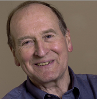 Henry Smith合作论文数Department of Electrical Engineering and Computer Science, Massachusetts Institute of Technology1
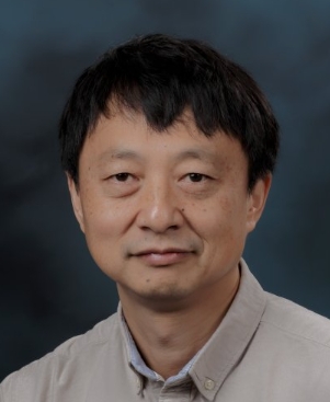 Frank Liu合作论文数School of Data Science, Old Dominion University;Texas A&M University1T. E. Mckoy合作论文数1Jin Woo Hong合作论文数Department of Electrical and Computer Engineering
Louisiana State University1
Frank Liu合作论文数School of Data Science, Old Dominion University;Texas A&M University1T. E. Mckoy合作论文数1Jin Woo Hong合作论文数Department of Electrical and Computer Engineering
Louisiana State University1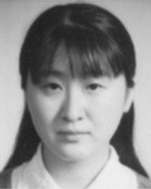 Haihua Su合作论文数1
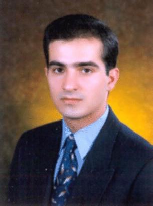 Soroush Abbaspour合作论文数University of Southern California1
 Michael W. Beattie合作论文数Department of Electrical and Computer Engineering, Carnegie Mellon University1B. K. Ko合作论文数1G. W. Mulvey合作论文数1
 Debjit Sinha合作论文数Google1H. H. Smith合作论文数1
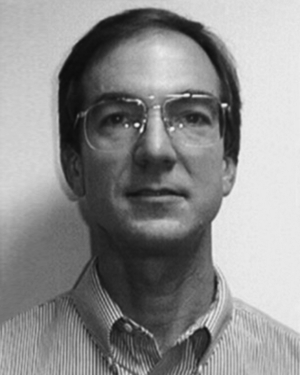 Paul Villarrubia合作论文数IBM Corporation, Austin, TX1John Magerlein合作论文数1
 Mathews Thomas合作论文数IBM1M. Scontras合作论文数1




