Alkali-based semiconductor photocathodes are extensively used as electron sources and photon detectors. The performance characteristics, such as quantum efficiency and thermal emittance, are fundamentally influenced by the properties of these materials, including crystallinity and surface roughness. Epitaxial growth of alkali-based photocathodes can be achieved on latticematched substrates using controlled growth techniques like molecular-beam epitaxy. At BNL, high quantum efficiency, ultrasmooth, and epitaxial thin film photocathodes of $\mathrm{K}_{2} \mathrm{CsSb}, \mathrm{Cs}_{3} \mathrm{Sb}$ and Cs2Te were developed on various latticematched substrates, utilizing in situ and real time synchrotron x-ray characterization techniques to gain insights into the stoichiometry, surface roughness and crystal structure of the photocathode materials.
The performance of electron accelerators and photon detectors heavily depends on the efficiency and stability of the photocathode. The emitted beam current and brightness can be limited by surface and bulk disorder in polycrystalline photocathode materials. Epitaxial growth offers a promising route to mitigate these limitations and enable high-current, high-brightness electron beams. In this work, we present the first demonstration of the epitaxial growth of a bi-alkali antimonide photocathode, K2CsSb, utilizing both pulsed laser deposition-assisted and thermal evaporation techniques. In our study, the growth of the epitaxial layer with a flat surface was confirmed by reflection high-energy electron diffraction for the K2CsSb thin film. In situ and real-time x-ray characterization were utilized to confirm the film stoichiometry, surface roughness, and crystallinity. Quantum efficiency (QE) of 3% at 530 nm and 9% at 450 nm was obtained from an epitaxial K2CsSb thin film with a film thickness as thin as 6 nm with an ultrasmooth surface of 0.4 nm roughness on a Gr/4H–SiC substrate. Increasing the thickness to 20 nm enhanced the QE to 4.5% and 14.5% at 530 and 450 nm, respectively, with the surface roughness remaining under 1 nm. In a follow-up experiment, QE of over 9% (530 nm) and 21% (450 nm) were achieved from an epitaxial K2CsSb thin film grown on a 4H–SiC single-crystal substrate.
Alkali antimonides are well established as high efficiency, low intrinsic emittance photocathodes for accelerators and photon detectors. However, conventionally grown alkali antimonide films are polycrystalline with surface disorder and roughness that can limit achievable beam brightness. Ordering the crystalline structure of alkali antimonides has the potential to deliver higher brightness electron beams by reducing surface disorder and enabling the engineering of material properties at the level of atomic layers. In this report, we demonstrate the growth of ordered Cs3Sb films on single crystal substrates 3C-SiC and graphene-coated 4H-SiC using pulsed laser deposition and conventional thermal evaporation growth techniques. The crystalline structures of the Cs3Sb films were examined using reflection high energy electron diffraction and x-ray diffraction diagnostics, while film thickness and roughness estimates were made using x-ray reflectivity. With these tools, we observed ordered domains in less than 10 nm thick films with quantum efficiencies greater than 1% at 530 nm. Moreover, we identify structural features such as Laue oscillations indicative of highly ordered films. We found that Cs3Sb films grew with flat, fiber-textured surfaces on 3C-SiC and with multiple ordered domains and sub-nanometer surface roughness on graphene-coated 4H-SiC under our growth conditions. We identify the crystallographic orientations of Cs3Sb grown on graphene-coated 4H-SiC substrates and discuss the significance of examining the crystal structure of these films for growing epitaxial heterostructures in future experiments.
The development of high-brightness electron sources is critical to state-of-the-art electron accelerator applications like X-ray free electron laser (XFEL) and ultra-fast electron microscopy. Cesium telluride is chosen as the electron source material for multiple cutting-edge XFEL facilities worldwide. This manuscript presents the first demonstration of the growth of highly crystalized and epitaxial cesium telluride thin films on 4H-SiC and graphene/4H-SiC substrates with ultrasmooth film surfaces. The ordering of the film was characterized by in situ reflection high energy electron diffraction and multiple X-ray diagnostics. The results of the quantum efficiency performance for epitaxial cesium telluride photocathodes are also reported.
Using in situ synchrotron X-ray diffraction, we interrogate the microstructural and phase evolution of polycrystalline nickel (Ni) during redox cycling in O2, H2, and H2O environments. Oxidation in O2 promotes strong (111) texturing in both the NiO overlayer and the underlying Ni substrate. However, this crystallographic alignment is lost following reduction in H2 and subsequent reoxidation, demonstrating irreversible microstructural changes. H2 exposure leads to proton dissolution into the Ni lattice, triggering a localized phase transition from face-centered cubic (FCC) to hexagonal close-packed (HCP) Ni in hydrogen-saturated regions. In H2O-containing atmospheres, dissociative H2O adsorption produces protons that permeate the NiO layer, forming γ-NiOOH within the NiO lattice and HCP Ni beneath the NiO overlayer as protons accumulate. Kinetic analysis via the Johnson-Mehl-Avrami-Kolmogorov model uncovers distinct growth mechanisms: preoxidized Ni surfaces follow one-dimensional (1D) kinetics for NiO, γ-NiOOH, and HCP growth, whereas pristine Ni exhibits three-dimensional (3D) kinetics due to island-like nucleation and growth of NiO. These results highlight the critical interplay between H2O dissociation, hydrogen permeation, and redox-driven phase transformations, with practical implications in engineering nickel-based catalysts and hydrogen storage systems through controlled microstructural and phase evolution.
Ultra-flat, ultra-thin alkali antimonide photocathodes with high crystallinity can exhibit high quantum efficiency and low mean transverse energy of outgoing electrons, which are essential requirements for a variety of applications for photocathode materials. Here, we investigate the growth of Cs3Sb on graphene-coated 4H–SiC (Gr/4H–SiC), 3C–SiC, and Si3N4 substrates. Sb is deposited using pulsed laser deposition, while Cs is deposited thermally and simultaneously. We demonstrate, employing x-ray analysis and quantum efficiency measurements, that this growth method yields atomically smooth Cs3Sb photocathodes with a high quantum efficiency (>10%), even in the ultra-thin limit (<30 nm). For the Si3N4 substrate, film growth is shown to be polycrystalline, while films grown on Gr/4H–SiC show a high degree of ordering with signs of epitaxy.
The electronic origin of the structural transition in 1T-VSe_2 is re-evaluated through an extensive angle-resolved photoemission spectroscopy experiment. The components of the band structure, missing in previous reports, are revealed. Earlier observations, shown to be temperature independent and therefore not correlated with the phase transition, are explained in terms of the increased complexity of the band structure close to the Fermi level. Only the overall size of the Fermi surface is found to be positively correlated with the phase transition at 110 K. These observations, quite distant from the charge density wave scenario commonly considered for 1T-VSe_2, bring fresh perspectives toward the correct description of structural transitions in dichalcogenides materials.
A new polytype of WTe2 with a bandgap has been recently discovered through the intercalation of lithium into the van der Waals gaps of Td- WTe2. Here, we report the effects of reduced thicknesses and heterointerfaces on the intercalation -induced phase transition in WTe2. Using in situ Raman spectroscopy during the electrochemical lithiation of WTe2 flakes as a function of flake thickness, we observe that additional electrochemical energy is required for the phase transition of WTe2 from the T-d phase to the new lithiated T-d ' phase, going from 0.8 V of the applied electrochemical voltage for a thick flake to 0.5 V and 0.3 V for 7- and 5layered samples, respectively. We ascribe this suppression of the phase transition to the interfacial interaction between the nanoflake and SiO2/Si substrate, which plays an increasing role as the sample thickness is reduced. The suppressed kinetics of the phase transition can be mitigated by placing the WTe2 flake on a hexagonal boron nitride (hBN) flake, which facilitates the release of the in -plane strain induced by the phase transition. Our study underscores the significance of interfacial effects in modulating phase transitions in two-dimensional (2D) materials, suggesting heterogeneous transition pathways, as well as interfacial engineering to control these phase transitions.
Multiple polytypes of MoTe2 with distinct structures and intriguing electronic properties can be accessed by various physical and chemical approaches. Here, we report electrochemical lithium (Li) intercalation into 1T'-MoTe2 nanoflakes, leading to the discovery of two previously unreported lithiated phases. Distinguished by their structural differences from the pristine 1T' phase, these distinct phases were characterized using in situ polarization Raman spectroscopy and in situ single-crystal X-ray diffraction. The lithiated phases exhibit increasing resistivity with decreasing temperature, and their carrier densities are two to 4 orders of magnitude smaller than the metallic 1T' phase, as probed through in situ Hall measurements. The discovery of these gapped phases in initially metallic 1T'-MoTe2 underscores electrochemical intercalation as a potent tool for tuning the phase stability and electron density in two-dimensional (2D) materials.
Periodic lattice distortion, known as the charge density wave, is generally attributed to electron–phonon coupling. This correlation is expected to induce a pseudogap at the Fermi level in order to gain the required energy for stable lattice distortion. The transition metal dichalcogenide 1T-VSe2 also undergoes such a transition at 110 K. Here, we present detailed angle-resolved photoemission spectroscopy experiments to investigate the electronic structure in 1T-VSe2 across the structural transition. Previously reported warping of the electronic structure and the energy shift of a secondary peak near the Fermi level as the origin of the charge density wave phase are shown to be temperature independent and hence cannot be attributed to the structural transition. Our work reveals new states that were not resolved in previous studies. Earlier results can be explained by the different dispersion natures of these states and temperature-induced broadening. Only the overall size of the Fermi surface is found to change across the structural transition. These observations, quite different from the charge density wave scenario commonly considered for 1T-VSe2 and other transition metal dichalcogenides, bring fresh perspectives toward correctly describing structural transitions. Therefore, these new results can be applied to material families in which the origin of the structural transition has not been resolved.
Transition metal dichalcogenides exhibit many fascinating properties including superconductivity, magnetic orders, and charge density wave. The combination of these features with a non-trivial band topology opens the possibility of additional exotic states such as Majorana fermions and quantum anomalous Hall effect. Here, we report on photon-energy and polarization dependent spin-resolved angle-resolved photoemission spectroscopy experiments on single crystal 1T-VSe 2 , revealing an unexpected band inversion and emergent Dirac nodal arc with spin-momentum locking. Density functional theory calculations suggest a surface lattice strain could be the driving mechanism for the topologically nontrivial electronic structure of 1T-VSe 2 .
This paper presents the results of experimental and theoretical studies of the effects of pressure and thermal annealing on the photo-conversion efficiencies (PCEs) of polymer solar cells with active layers that consist of a mixture of poly(3-hexylthiophene-2,5-diyl) and fullerene derivative (6,6)-phenyl-C61-butyric acid methyl ester. The PCEs of the solar cells increased from ∼2.3% (for the unannealed devices) to ∼3.7% for devices annealed at ∼150 °C. A further increase in thermal annealing temperatures (beyond 150 °C) resulted in lower PCEs. Further improvements in the PCEs (from ∼3.7% to ∼5.4%) were observed with pressure application between 0 and 8 MPa. However, a decrease in PCEs was observed for pressure application beyond 8 MPa. The improved performance associated with thermal annealing is attributed to changes in the active layer microstructure and texture, which also enhance the optical absorption, mobility, and lifetime of the optically excited charge carriers. The beneficial effects of applied pressure are attributed to the decreased interfacial surface contacts that are associated with pressure application. The implications of the results are then discussed for the design and fabrication of organic solar cells with improved PCEs.
We demonstrate the key features of an interference cathode using both simulations and experiments. We deposit Cs3Sb photocathodes on Ag to produce an interference enhanced photocathode with 2–5× quantum efficiency (QE) enhancement using a robust procedure that requires only a smooth metal substrate and QE monitoring during growth. We grow both an interference cathode (Ag substrate) and a typical photocathode (Si reference substrate) simultaneously to confirm that the effects are due to optical interactions with the substrate rather than photocathode composition or surface electron affinity differences. Growing the cathodes until the QE converges shows both the characteristic interference peaks during growth and the identical limiting case where the cathode is “infinitely thick,” in agreement with simulations. We also grow a cathode until the QE on Ag peaks and then stop the growth, demonstrating broadband QE enhancement.
The ion-induced nanoscale pattern formation on a crystalline Ge(001) surface is observed in situ by means of grazing incidence small angle x-ray scattering (GISAXS). Analysis of the GISAXS intensity maps yields the temporal development of geometric parameters characterizing the changing pattern morphology. In comparison with theoretical predictions and with simulations of the patterning process based on a continuum equation we find good agreement for the temporal evolution of the polar facet angle, characteristic length, and surface roughness in the nonlinear regime. To achieve this agreement, we included an additional term in the continuum equation which adjusts the pattern anisotropy.
A commentary is provided on a new type of prism deflection scanning X-ray microscope, providing context and some future potential applications of this new type of microscope.
Pulsed laser deposition (PLD) is widely used to grow epitaxial thin films of quantum materials. Here, we use in situ x-ray scattering to study homoepitaxy of SrTiO3 by energetic deposition (e-PLD) versus PLD thermalized by a He background gas (th-PLD). Energetic PLD suppresses the lateral growth of two-dimensional islands, which suggests that particles with kinetic energies of similar to 100 eV break up smaller islands. Fast interlayer transport occurs for th-PLD as well as e-PLD, implying a process operating on submicrosecond time scales for incident particles with kinetic energies below 10 eV.
In ferroelectric thin films and superlattices, the polarization is intricately linked to crystal structure. Here we show that it can also play an important role in the growth process, influencing growth rates, relaxation mechanisms, electrical properties and domain structures. This is studied by focusing on the properties of BaTiO 3 thin films grown on very thin layers of PbTiO 3 using x-ray diffraction, piezoforce microscopy, electrical characterization and rapid in-situ x-ray diffraction reciprocal space maps during the growth using synchrotron radiation. Using a simple model we show that the changes in growth are driven by the energy cost for the top material to sustain the polarization imposed upon it by the underlying layer, and these effects may be expected to occur in other multilayer systems where polarization is present during growth. This motivates the concept of polarization engineering as a complementary approach to strain engineering.
A useful way to study a wide range of materials with ordered and disordered phases at high pressures is With the X-ray Pair Distribution Function (PDF) method. Typically one uses a Diamond Anvil Cell (DAC) to create the high pressure environment for the sample. High quality X-ray PDF data is best obtained by using high energy photons, preferably 50 KeV and higher. In a DAC, the small sample volumes and the close proximity of the gasket material to the sample motivates the use of focusing lenses to increase the Ilux density of photons on the sample, while simultaneously decreasing the flux density on the gasket. We investigate the use of kinofonn lenses for this application of X-Ray PDF in a Diamond Anvil Cell.
Pulsed Laser Deposition (PLD) is widely used to grow epitaxial thin films of quantum materials such as complex oxides. Here, we use in-situ X-ray scattering to study homoepitaxy of SrTiO$_3$ by energetic (e-) and thermalized (th-) PLD. We find that e-PLD suppresses the lateral growth of two-dimensional islands, which suggests that energetic particles break up smaller islands. Fast interlayer transport occurs for both e-PLD and th-PLD, implying a process operating on sub-microsecond timescales that doesn't depend strongly on the kinetic energy of the incident particles.
Ecological pressures and varied feeding behaviors in a multitude of organisms have necessitated the drive for adaptation. One such change is seen in the feeding appendages of stomatopods, a group of highly predatory marine crustaceans. Stomatopods include “spearers,” who ambush and snare soft bodied prey, and “smashers,” who bludgeon hard‐shelled prey with a heavily mineralized club. The regional substructural complexity of the stomatopod dactyl club from the smashing predator Odontodactylus scyllarus represents a model system in the study of impact tolerant biominerals. The club consists of a highly mineralized impact region, a characteristic Bouligand architecture (common to arthropods), and a unique section of the club, the striated region, composed of highly aligned sheets of mineralized fibers. Detailed ultrastructural investigations of the striated region within O. scyllarus and a related species of spearing stomatopod, Lysiosquillina maculate show consistent organization of mineral and organic, but distinct differences in macro‐scale architecture. Evidence is provided for the function and substructural exaptation of the striated region, which facilitated redeployment of a raptorial feeding appendage as a biological hammer. Moreover, given the need to accelerate underwater and “grab” or “smash” their prey, the spearer and smasher appendages are specifically designed with a significantly reduced drag force.
 Aaron Stein合作论文数Ctr Funct Nanomat, Brookhaven Natl Lab17
 Martin L. Green合作论文数National Institute of Standards and Technology, National Institute of Standards and Technology10
 Tang M T合作论文数9
 Steven Cundiff合作论文数Department of Physics, University of Michigan6
 Frieder Heinrich Baumann合作论文数5Smedley John合作论文数Brookhaven Natl Lab5
 Mengjia Gaowei合作论文数Graduate University of Chinese Academy of Sciences, Graduate University of Chinese Academy of Sciences5James Michael Ablett合作论文数Experimental Division, Synchrotron SOLEIL5T Sorsch合作论文数5k s krisch合作论文数5Daniel A. Steingart合作论文数4l manchanda合作论文数4Ashley Taylor合作论文数4Greg Bogart合作论文数4
 Siddharth Karkare合作论文数Department of Physics, Arizona State University4Donald M. Tennant合作论文数4Gs Higashi合作论文数4
 Jared Maxson合作论文数Department of Physics, College of Arts and Sciences, Cornell University4
 Chris Jacobsen合作论文数Department of Physics & Astronomy, Weinberg College of Arts & Sciences, Northwestern University4Hertzberg Benjamin合作论文数Woodruff School of Mechanical Engineering, Georgia Institute of Technology4
 Steven Herrera合作论文数Department of Chemical and Environmental Engineering, University of California, Riverside4
 Garrett Milliron合作论文数Department of Chemical and Environmental Engineering, University of California, Riverside4
 Pablo Daniel Zavattieri合作论文数Lyles School of Civil Engineering, Purdue University4Fred Klemens合作论文数4
 Randall L. Headrick合作论文数Department of Physics, University of Vermont4
 A. R. Sandy合作论文数Advanced Photon Source;Argonne National Laboratory;Argonne National Laboratory4Daniel R. Brasen合作论文数4
 David Kisailus合作论文数Department of Molecular;Cellular and Developmental Biology;Institute for Collaborative Biotechnologies;Materials Research Laboratory;University of California , Santa Barbara;Institute for Collaborative Biotechnologies, University of California , Santa Barbara4
 Alastair MacDowell合作论文数Lawrence Berkeley National Laboratory4Yu-chen Karen Chen-Wiegart合作论文数3Scott Ustin合作论文数3Harold Huggins合作论文数3
 Isaias Gallana合作论文数3M. E. Gross合作论文数3Hassaram Bakhru合作论文数3Turgut Yilmaz合作论文数3Jeffrey G. Ulbrandt合作论文数Univ Vermont, Dept Phys, Burlington, VT 05405 USA3Rui Liu合作论文数3Patrizia Imperatori合作论文数3Yaraghi Nicholas合作论文数Department of Chemical and Biomolecular Engineering, University of Maryland3
 Lessa Grunenfelder合作论文数Mork Family Department of Chemical Engineering & Materials Science, School of Engineering, University of Southern California, Riverside3
 Wang Jun合作论文数3
 Gaikwad Abhinav M合作论文数CUNY Energy Institute, The City College of New York3
 James R. Fienup合作论文数The Institute of Optics, Hajim School of Engineering & Applied Sciences, University of Rochester;Laboratory for Laser Energetics, University of Rochester;Center for Visual Science, University of Rochester3
 Sanjoy Banerjee合作论文数Energy Institute, The City University of New York;Department of Chemical Engineering, The Grove School of Engineering, The City College of New York;Urban Electric Power3T. Boone合作论文数3
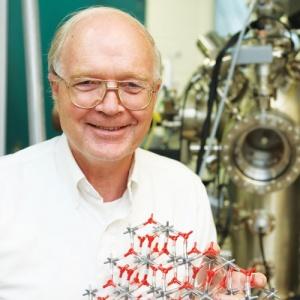 Richard M. Osgood合作论文数Department of Applied Physics and Applied Mathematics, Columbia University3
 Gregory Timp合作论文数College of Engineering, University of Notre Dame3
 Rudolf M. Tromp合作论文数T.J Watson Research Center, IBM/Leiden University3




