Developing high efficient and stable non-noble metal catalyst for water electrolysis is particularly crucial. Herein, we reported B-doped FeCoNi (Oxy) Hydroxides (FeCoNiB) on the surface of Ni foam substrate (NF) synthesized through a facile and mild two-step strategy of electrodeposition followed by impregnation. This synthesis strategy can efficiently introduce surface defects by B doping to FeCoNi (Oxy) Hydroxides while maintaining its original morphology. The obtained FeCoNiB/NF catalyst displayed an unique three-dimensional (3D) flower-like cluster architecture composed of thin nanosheets. The FeCoNiB/NF exhibited outstanding OER electrocatalytic activity, requiring the low overpotential of only 308 mV to achieve the current density of 100 mA cm-2 with the low Tafel slope of 59.0 mV dec-1. The enhanced catalytic activity of FeCoNiB/NF is mainly attributed to the synergistic enhancement effect of high-valence Fe and Co, surface defect, and amorphous-crystalline interfaces. When FeCoNiB/NF was employed as the anode catalyst for overall water electrolysis, it requires only 1.62V to achieve 20 mA cm-2, and operates stably for over 50 h, verifying its great potential applicability. This work provides an effective strategy for the design of high-performance non-noble metal electrocatalyst for water electrolysis.
In 2024, the MOE Key Laboratory of Macromolecular Synthesis and Functionalization at Zhejiang University continued its impactful researches across five core areas. In controllable catalytic polymerization, organoboron catalysts were developed for CO2 copolymerization and novel photoresist materials. Studies in microstructure and rheology elucidated universal deformation modes in graphene-based 2D membranes and improved graphene fiber properties through shear alignment engineering, defect control, and enhanced interlayer entanglement. For separating functional polymers, Janus membranes and channels were created for multiphase separation, liquid-phase molecular layer-by-layer deposition technique was developed to fabricate aromatic polyamide nanofilms, and the harmonic amide bond density was established as a valuable parameter for polyamide structural analysis. In biomedical functional polymers, a sustainable carboxyl-ester transesterification strategy was proposed for upcycling poly(ethylene terephthalate) (PET) waste into biodegradable plastics. Additionally, immunocompatible biomaterials were designed utilizing zwitterionic polypeptides and albumin-derived coatings, and Cu2 + -phenolic nanoflower was designed to combat fungal infections by combining cuproptosis and cell wall digestion. Further, the researchers developed a gelatin-DOPA-knob/fibrinogen hydrogel to achieve rapid and robust hemostatic sealing, utilized a double-network polyelectrolyte-coated hydrogel for enhancing endothelialization of left atrial appendage (LAA) occluders, and the researchers also demonstrated that image-guided highintensity focused ultrasound enables manipulation of shape-memory polymers. Finally, in the realm of photo-electro-magnetic functional polymers, precise control of through-space conjugation was shown to enhance organic luminescence. Topologically structured hydrogels were revealed to exhibit autonomous actuation. Also, solar-driven photothermal ion pumps were developed for selective lithium extraction from seawater, and high-performance non-solvated C60 single-crystal films were prepared via facile bar coating. Lastly, the researchers demonstrated outstanding dielectric properties of polyethylene (PE) lamellar single crystals. The relevant works are reviewed in this paper. (c) 2025 Published by Elsevier B.V. on behalf of Chinese Chemical Society and Institute of Materia Medica, Chinese Academy of Medical Sciences.
Meniscus-guided coating (MGC) enables facile production of large-area, unidirectionally oriented organic semiconductor crystalline thin-films. While efforts have been made in controlling the morphology of MGC-grown films, leading to improvements in device performance and uniformity along the coating direction, film continuity perpendicular to the coating direction has been largely overlooked. This work demonstrates that using high surface tension solvents significantly improved film continuity in the direction perpendicular to the coating, which was applicable to various organic semiconductors. Specifically, 6,13-bis(triisopropylsilylethynyl)pentacene (TIPS-PEN) film exhibited millimeter-sized domains and effective grain boundary contact, displaying single-crystal-like charge transport properties. Organic field-effect transistor arrays based on this two-dimensionally continuous, oriented crystalline thin-film showed enhanced mobilities and device-to-device uniformity in both parallel and perpendicular directions to the coating. The lowest coefficient of variation, 5.0%, was obtained for TIPS-PEN. This work provides a universal strategy for improving the continuity of MGC-grown films, promoting the practical application of organic semiconductor single crystals (OSSCs) in organic electronics.
Self-assembled monolayers (SAMs) offer a powerful molecular-level approach to tuning the interface between indium tin oxide (ITO) anode and active layer in organic solar cells (OSCs). To realize better interfacial modification, herein, site-specific fluorinations of a kind of SAM material with 9,10-dihydro-9,9-diphenylacridine as the conjugated head are performed. Two fluorinated derivatives and their nonfluorinated parent compound, named 4PA-FPhAc, 4PA-PhAcF, and 4PA-PhAc, are synthesized. It is found that 4PA-FPhAc, containing fluorine atoms at the para-positions of the phenyl side chains on the acridine ring, exhibits stronger binding with ITO, enhanced intermolecular interactions, and a tendency to form a denser and more homogeneous molecular assembly, leading to improved interfacial energetic alignment and more efficient hole extraction. In contrast, fluorinations on the acridine backbone perturb molecular packing of 4PA-PhAcF and deteriorate interfacial contact. As a result, binary OSCs incorporating 4PA-FPhAc deliver an impressive efficiency of 19.56%, outperforming counterparts adopting 4PA-PhAc (18.78%) and 4PA-PhAcF (11.90%). Notably, 20.25 cm2 photovoltaic modules with the SAM of 4PA-FPhAc provide a high efficiency of 16.97%. This work demonstrates that site-selective fluorination is an effective molecular-tailoring strategy for high-quality SAMs applicable in OSCs.
Polymer lamellar crystals with highly ordered crystalline structures are ideal systems for understanding and engineering thermally conductive polymers. However, their nanometer-scale thickness, hard-to-eliminate defects, and limited lateral dimensions have impeded experimental characterization, leaving key thermal transport mechanisms unresolved. Here, we address this knowledge gap by devising a multilayer single-crystal stack for a non-contact measurement technique, combined with advanced theoretical calculations. The measured cross-plane thermal conductivity is 4 W m-1 K-1 for a 12-nm-thick polyethylene lamellar single crystal, representing the highest value observed for dielectric materials in this thickness range. Theoretical analyses indicate that this value is nevertheless limited by the combined effects from boundary scattering and surface amorphization, offering critical insights for molecular design and understanding of nanoscale heat transfer in ultrathin soft materials.
Bulk heterojunction (BHJ) active layers in organic photovoltaics (OPVs) are nanostructured composites in which electron-donating and electron-accepting semiconductors form interpenetrating phases for exciton dissociation and charge transport. The power conversion efficiency (PCE) of these organic-organic nanocomposites is governed by structural features spanning multiple length scales: molecular packing and energy-level alignment at donor/acceptor (D/A) interfaces, phase-separation morphology and crystallite connectivity, and thin-film optical and charge-transport characteristics. Rational design of high-performance OPV nanocomposites requires multiscale numerical modelling that bridges quantum chemistry, mesoscale morphology simulation, and device-scale optoelectronic modelling. This review surveys and critically compares recent advances in the structural design and numerical simulation of OPV BHJ nanocomposites. At the molecular scale, we examine density functional theory and non-adiabatic molecular dynamics approaches for resolving charge-separation driving forces, interfacial energy-level alignment, and exciton dynamics. At the mesoscale, we discuss molecular dynamics, kinetic Monte Carlo, and electronic coarse-graining methods for describing phase separation, crystallization kinetics, morphology evolution, and charge transport. At the device scale, we review exciton-diffusion, optical transfer-matrix, and drift-diffusion models that quantitatively link morphology to photovoltaic performance metrics. The review also evaluates how machine learning, high-throughput screening, surrogate models, and generative design accelerate donor-acceptor selection and morphology optimization, while distinguishing benchmark predictions from experimentally validated design rules. Across these scales, we compare the strengths, assumptions, and validation limits of the principal modelling approaches. Finally, we highlight emerging multiscale integration frameworks, including sequential parameter-passing pipelines and differentiable digital-twin concepts. By framing OPV BHJ layers as nanocomposites whose performance bottlenecks map onto composite-design challenges such as interface integrity, phase connectivity, multiscale charge transfer, and degradation-aware design, this review connects OPV modelling with broader structural-composites thinking for next-generation organic solar cells.
Organic semiconductor single crystals (OSSCs), which possess the inherent merits of long-range order, low defect density and absence of grain boundaries, hold tremendous potential for achieving high-performance organic field-effect transistors (OFETs). Nevertheless, OSSCs remain in the early stages of implementation for organic circuits. A critical bottleneck is the lack of reliable patterning methods capable of yielding single-crystal arrays with high mobility and uniformity. Herein, a dry-transfer patterning strategy is developed, in which the molecularly flat surface is preserved. Consequently, the dry-transfer patterned C8-DNTT molecular monolayer crystals (MMCs) deliver exceptional electrical properties, featuring a high intrinsic mobility of 16.80 cm2 V−1 s−1 and a low contact resistance of 44.36 Ω cm. These pristine channels enable the construction of high-performance unipolar inverters, achieving a high gain of 60 and a noise margin of 56% VDD/2. With the preserved high mobility and outstanding uniformity within one single-crystalline domain of C8-DNTT MMCs, five-stage ring oscillators are successfully integrated and exhibit a signal propagation delay of 0.71 ms. Overall, this work provides a promising strategy for building organic integrated circuits with singular OSSCs.
ABSTRACT Organic light‐emitting transistors (OLETs) have great potential in the next‐generation display technology. However, achieving uniform emission remains a challenge. In this study, monolayer molecular crystals (MMCs) of C 5 ‐DNTT were developed as highly efficient bi‐functional active layers for area‐emitting OLETs, providing a mobility of 6.64 cm 2 V −1 s −1 , threshold voltage of −0.46 V, current on/off ratio over 10 6 , and subthreshold swing of 226 mV/dec. The C 5 ‐DNTT MMC‐based OLETs exhibit a uniform emission across the entire anode region, with the intensity difference between the two edges of the emitting area smaller than 6.8%. Compared to polycrystalline thin‐film OLETs, the C 5 ‐DNTT MMC‐based OLETs achieve a transition from typical line emission to area emission, thanks to the efficient horizontal hole transport and vertical hole injection. This work demonstrates the potential of high‐mobility MMCs as the bi‐functional hole transport and injection layers in high‐performance OLETs, offering novel insights for developing uniform area‐emitting OLETs and facilitating the application of OLETs in future displays.
Hierarchical spherulite structures are ubiquitous in semicrystalline polymers and impact their properties. Elucidating these delicate and complex structures, which span from molecular-level chain folding to mesoscale spherulites, however, presents a formidable challenge. Here, we showcase low-dose four-dimensional (4D) scanning transmission electron microscopy (STEM) as a powerful technique for investigating the multiscale hierarchical structures of polymer spherulites. Applying it to poly(ε-caprolactone) and polyethylene (PE) spherulite films, we reveal the preferential orientation and growth direction of lamellar crystals, as well as the twisted lamella structure in PE banded spherulites. Notably, our observations reveal a non-radial twisting axis forming a spiral texture in PE films. With the enhanced spatial resolution of cryogenic 4D-STEM, we directly visualize individual lamellar crystals at the nanoscale, enabling the identification of chain tilt within a single lamella and the elucidation of lamella configurations at spherulite boundaries. These insights advance our understanding of polymer spherulite crystallization mechanisms and underscore low-dose 4D-STEM as a powerful tool for exploring the intriguing structures of soft materials.
The macroscopic properties of polymer-based low-dimensional nanomaterials are intrinsically governed by their dimensions. Achieving full-dimensional tunability is thus paramount for precise control over their bulk performance. While the planar dimensions of two-dimensional nanomaterials are often adjustable, precise control over their thickness, a parameter associated with chain packing in the nongrowth direction, remains challenging due to thermodynamic and kinetic constraints. Herein, we construct a library of semicrystalline polymers bearing long crystallizable alkyl side chains on flexible, semirigid, and rigid backbones to systematically investigate how side-chain length affects crystallization behavior. Among them, cyclopentene-based polymers (CPs) serve as the representative model system for establishing the quantitative correlation between side-chain length and crystal thickness. Through a multitechnique characterization approach, we elucidate the correlation between side-chain length and crystal thickness, laying a foundation for achieving fully tunable dimensions in polymeric nanomaterials.
Using the gel-grown method to control the morphology of crystals attracts extensive attention. Potassium dihydrogen phosphate (KDP) is a nonlinear optical crystal with a high laser damage threshold. Here, we studied the crystallization of KDP in silica gel. The kebab-like KDP crystals (multiple KDP crystals aligning along a straight line) were prepared in the silica gel. In situ observation revealed that the kebab-like crystals were obtained through secondary nucleations on preformed needle-like crystals. Further investigation revealed that the hydroxyl groups on the gel network have an important influence on the formation of kebab-like KDP crystals. The hydroxyl groups on the gel networks can form hydrogen bonds with the phosphoric acid group of the KDP crystal and hinder the growth of the prismatic KDP faces, which leads to the preformation of needle-like crystals. Additionally, the influence of the acetic acid concentration and antisolvent on morphology was also studied.
Charge-transfer complexes (CTCs) have emerged as promising n-type organic thermoelectric (TE) materials due to their inherent high electrical conductivity and tunable transport polarities. In this study, we performed a comprehensive first-principles investigation on the TE properties of nine CTCs comprised of 2,7-dialkyl[1]benzothieno[3,2-b][1]benzothiophenes (CnBTBT, n = 4, 8, 12) as donors and fluorinated derivatives of tetracyanoquinodimethane (FmTCNQ, m = 0, 2, 4) as acceptors, aiming to identify highperformance n-type organic TE materials and elucidate the underlying structure-property relationships. Our calculation results, based on the Boltzmann transport equation and deformation potential theory, reveal that the length of the alkyl side chains and the number of fluorine substitutions significantly impact their electronic structures and TE properties. Notably, the CnBTBT-FmTCNQ CTCs with shorter alkyl chains and more fluorine substitution demonstrate superior n-type characteristics, particularly C4BTBT-F4TCNQ, which achieves an excellent power factor of 671 mu W cm-1 K-2 at an optimal charge carrier concentration. Our findings not only clarify the critical role of molecular engineering in CTC-based TE materials but also provide valuable guidance for developing high-efficiency organic TE materials with versatile practical applications. (c) 2025 Published by Elsevier B.V. on behalf of Chinese Chemical Society and Institute of Materia Medica, Chinese Academy of Medical Sciences.
The recyclability and reuse of polymeric materials have become increasingly necessary. Introducing depolymerizability or degradability into polymers without compromising the mechanical performance but concurrently endowing the polymers with new properties is challenging. In this contribution, a family of polypentenamers with different alkyl side chains ranging from nonyl to octacosyl were synthesized. The polycyclopentene backbone provides polymer depolymerizability, promoting degradation into their original building blocks, which also can repolymerize into polymers, realizing full closed-loop recycling. Crystalline side chains help afford polyethylene-like strength and modulus. The lamellar thickness of sub-5 nm can be precisely controlled. Inserting an ethylene glycol unit along the side chain allowed them to be easily transferred into 10 kinds of new polyolefins with various functions. These degradable polycyclopentene-backboned polymers with crystalline pendants pave sustainable ways for the recyclability and reuse of polyolefin materials for, for example, packaging applications.
Reported here is the synthesis of stretchable hydrogels with large spherulites of different morphologies by polymerization-induced crystallization of dopant molecules. By varying the concentrations of chemical crosslinker and initiator, or the light intensity for photopolymerization, the stiffness of polyacrylamide network is tunable to regulate the crystallization of dibenzo-24-crown-8-ether molecules that form spherulites in the hydrogels. Regular spherulites are formed in relatively stiff gels, whereas banded spherulites with twisted crystal fibers are obtained in soft gels. The structure of spherulites is investigated by microscopy and scattering measurements. The formation of twisted crystal fibers is related to dynamic variations of crystallization pressure and network impedance. The gels with regular spherulites show stronger fluorescence and phosphorescence than those with banded spherulites. A remarkable fact is that the latter gels exhibit circularly polarized luminescence (CPL) with dissymmetry factor up to +1.5 × 10⁻². This luminescence arises from the clusterization-triggered emission of the network constrained by the crystals, while the twisted fibers render the achiral clusterluminogens with CPL. The mutual influences between polymer network and crystal growth account for the collective functions of the composite gels. The design principle and chiral transfer mechanism should open opportunities for developing other soft materials with tailored crystals and optical properties.
The multiple-component strategy shows great potential in optimizing the performance of organic photovoltaics (OPVs), while the addition of extra components does not usually guarantee a positive effect on the already-perfected morphology of the binary blend, and thus results in an inferior device performance. To address this issue, we develop a facile dual-additive strategy to compensate the negative effect caused by extra components, and this allows the full exploitation of the multiple-component strategy toward a breakthrough in device performance. Specifically, by employing the dual additives of liquid additive 1,8-diiodooctane and solid additive 1,4-diiodobenzene, the film formation kinetics are optimized, and an optimal hierarchical morphology is formed with balanced crystallization, phase separation and prominent vertical distribution. Therefore, this dual-additive strategy leads to efficient exciton dissociation, charge transport, reduced exciton recombination and suppressed energy loss, offering great promise for high performance OPVs. Consequently, we reach a high efficiency of 20.52% (certified 19.92%) in single-junction OPVs. This work highlights the importance of morphology control for multi-component OPVs and sets a benchmark to accelerate their commercialization.
Quantum-dot light-emitting diodes (QLEDs) promise a new generation of low-cost, efficient, bright, and stable light sources. Achieving large-area patterning of high-resolution QLED arrays is essential for display applications. However, patterning of micro-QLEDs arrays via conventional photolithography, the most established and scalable technique capable of producing micrometer-scale patterns, poses challenges because the chemicals and solvents used can damage quantum dot emissive layers and charge transport layers (CTLs) during ultraviolet (UV) exposure and development. Here, we address these challenges by designing a novel hole transport layer (HTL), poly((9,9-dioctylfluorenyl-2,7-diyl)-co-(9-(2-ethylhexyl)-carbazole-3,6-diyl)-co-(9-(4-(4-vinylphenoxy)butyl)-carbazole-3,6-diyl)) (PF8Cz-X), which replaces reactive triphenylamine (TPA) units with chemically stable carbazole derivatives and introduces vinylphenoxy groups that crosslink upon annealing, enhancing solvent resistance. Utilizing PF8Cz-X, we fabricated efficient and high-resolution micro-QLEDs arrays with pixel sizes down to similar to 2 mu m, achieving resolutions up to 6000 pixels per inch. The red, green, and blue micro-QLEDs demonstrate peak external quantum efficiencies (EQEs) of 16.5%, 20.1%, and 12.7%, respectively, matching those of un-patterned devices. Our work reveals that conventional photolithography can be effectively employed for the fabrication of high-resolution micro-QLEDs array, paving the way towards advanced display applications in augmented reality (AR) and virtual reality (VR) technologies.
Polymer lamellar single crystals (PLSCs), the fundamental crystalline units of semicrystalline polymers, are ideal model systems to probe intrinsic structure-property relationships of polymer dielectrics. However, the reliable preparation and characterization of PLSCs remain challenging. Here, using a controlled solvent evaporation method, large-area isotactic poly(1-butene) (iPB-1) single crystals with lateral dimension spanning several hundred micrometers were directly grown on conductive substrates. This, in turn, enables straightforward fabrication of metal–insulator–metal (MIM) capacitors, and facilitates the subsequent determination of the dielectric constant for form III iPB-1 single crystals with a remarkably low value of 1.82 ± 0.05. This low value is attributed to suppressed chain-segmental motion and low molecular packing density of form III crystal phase. This study provides a model framework for quantifying the intrinsic dielectric performance of crystalline phase in semicrystalline polymer systems and highlighting the importance of crystal structure in determining the macroscopic behavior of polymeric dielectrics.
Organic semiconductor single crystals (OSSCs) hold promising prospects in high-performance organic field-effect transistors (OFETs) owing to the advantages of longrange ordering and few defects. However, until now, OSSCs have not shown their strength in flexible complementary integrated circuits, partly due to the lack of high-quality dielectric layers suitable for both large-area crystal growth by solution method and the construction of high-performance n-channel and p-channel transistors simultaneously. Herein, flexible OFETs are fabricated with solution-processed large-area OSSCs and dual-crosslinked bilayer dielectrics, in which the bottom high-k polymer provides key dielectric properties and the top low-k polymer offers improved semiconductor/dielectric interface. Thus, both n-channel and p-channel OFETs with high mobility (electron mobility of 1.97 cm2V-1s-1 and hole mobility of 11.97 cm2V-1s-1), low threshold voltage and subthreshold swing are realized with operation voltage of only 5 V, which lead to complementary inverters with a high gain of 59.8 and large noise margins reaching 75% of 1/2 VDD. Moreover, the devices exhibit great electrical bias-stress stability within 10,000 s, and mechanical flexibility with bending stability up to 10,000 cycles. This efficient manufacturing method of flexible OFETs and complementary inverters with large-area OSSC films and bilayer dielectric paves the way toward high-performance and low-power-consumption flexible circuits.
In conventional semiconductors, electrical and thermal conductivity are typically coupled, posing a challenge in optimizing both simultaneously. Overcoming this inherent trade-off enables strategies for advancing electronic applications. Herein, a strategy is demonstrated to decouple electrical and thermal conductivity trade-off by creating heterostructures of highly conductive single-walled carbon nanotubes (SWCNTs) coated with low conductivity hybrid perovskites. Coating SWCNTs with methylammonium lead iodide perovskite results in an enhancement in electrical conductivity (408-1266 S cm-1) due to p-type doping followed by a threefold decrease of the in-plane thermal conductivity (3.3-1 W m-1 K-1), compared to pristine SWCNTs. Molecular dynamics simulations uncover phonon boundary scattering at the SWCNT/perovskite interface as well as localization of methylammonium-related and softening of the Pb─I-related phonon modes in methylammonium lead iodide perovskite decreasing the thermal conductivity.
 Hongzheng Chen (陈红征)合作论文数Department of Polymer Science and Engineering, Zhejiang University91
) Pengxu Qian (钱鹏旭)合作论文数The First Affiliated Hospital, Zhejiang University School of Medicine;Liangzhu Laboratory, Zhejiang University33
Pengxu Qian (钱鹏旭)合作论文数The First Affiliated Hospital, Zhejiang University School of Medicine;Liangzhu Laboratory, Zhejiang University33 Yujing Liu (刘育京)合作论文数College of Chemistry and Life Science, Changchun University of Technology26
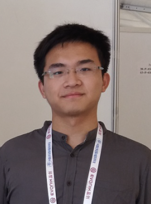 Jie Ren (任劼)合作论文数Organic Semiconductors Lab, Zhejiang University26
 Boyu Peng (彭博宇)合作论文数Department of Polymer Science and Engineering, Zhejiang University25
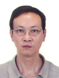 Minmin Shi (施敏敏)合作论文数Department of Polymer Science and Engineering, Zhejiang University20
 Wang Mang合作论文数20
 He Huang (黄河)合作论文数The First Affiliated Hospital, Zhejiang University School of Medicine;Zhejiang University Institute of Hematology20
 Min Chen合作论文数Dept Chem, Louisiana State Univ18Jiake Wu合作论文数18
 Tao Ye合作论文数Boeing17
 Weifei Fu (傅伟飞)合作论文数16
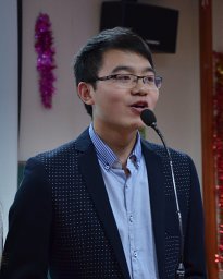 Guobiao Xue合作论文数MOE Key Lab Macromol Synth & Functionalizat, Zhejiang Univ14
 Xinyi Jin合作论文数14
 Penglei Jiang (姜蓬垒)合作论文数The First Affiliated Hospital, Zhejiang University School of Medicine13Fan Congcheng合作论文数13Huanbin Li合作论文数12
 Lara Estroff合作论文数Department of Materials Science and Engineering, Duffield College of Engineering, Cornell University11
 Huolin Xin合作论文数Department of Physics Astronomy, University of California, Irvine11Zhaoru Zhang合作论文数10Ruihan Wu合作论文数10
 Lijian Zuo (左立见)合作论文数Department of Polymer Science and Engineering, Zhejiang University10Wenchang Qian合作论文数9Shuang Liu合作论文数9
 Gang Wu (吴刚)合作论文数Department of Polymer Science and Engineering, Zhejiang University9
 Yujie Zhao合作论文数School of Physics and Astronomy, University of St Andrews9
 Jingzhi Sun (孙景志)合作论文数Department of Polymer Science and Engineering, Zhejiang University9Jinxin Li合作论文数8Zhuoting Huang合作论文数8
 Liao Chen合作论文数University of Notre Dame8
 Xinhui Lu (路新慧)合作论文数Department of Physics, The Chinese University of Hong Kong8
 Thomas H. LaBean合作论文数Department of Materials Science and Engineering, North Carolina State University8
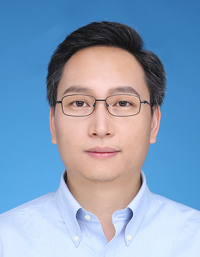 Chang-Zhi Li (李昌治)合作论文数Department of Polymer Science and Engineering, Zhejiang University8
 Hao Wei (魏浩)合作论文数School of Integrated Circuits, Shanghai Jiao Tong University8Zebin Yu合作论文数7Ling Wang合作论文数7Lingli Jiang合作论文数7Zhu Meng合作论文数7
 Ziliang Wu (吴子良)合作论文数Department of Polymer Science and Engineering, Zhejiang University7Yuhui Yang (阳禹辉)合作论文数6Xin Zeng合作论文数6
 Yongxian Hu (胡永仙)合作论文数The First Affiliated Hospital, Zhejiang University School of Medicine6Tianning Gu合作论文数6Qiwei Wang合作论文数6Dapeng Hu合作论文数6
 Shuixing Li (李水兴)合作论文数MOE Key Laboratory of Macromolecular Synthesis and Functionalization, Zhejiang University;Organic Semiconductors Lab, Zhejiang University6
 Zhenan Bao (鲍哲南)合作论文数Department of Chemical Engineering, Stanford University;Department of Materials Science and Engineering, Stanford University6
 Bao-Ku ZHU (朱宝库)合作论文数Department of Polymer Science and Engineering, Zhejiang University6Jiazhen Cui合作论文数5




