This paper presents a 5.4V-V in , 0.6-1.8V V out , 10MHz LDMOS-based buck IVR chiplet implemented in a 55nm BCD process featuring a self-timed bootstrap technique and same-cycle all-digital ZVS control to achieve 9.3A/mm 2 current density and 93.6% peak conversion efficiency, while meeting all reliability constraints. The IVR chip supports a maximum load current of 80A and occupies 8.6mm 2 die area.
High-performance computing for AI and supercomputing applications are pushing the power and performance envelopes exponentially in highly volume constrained environments. This market segment is driving up the complexity of systems on package (SoP) and, power delivery in conjunction with heat removal are emerging as dominant bottlenecks. These demand reticle sized dies, and the process yields often dictate disaggregated approaches where the SoP consists of numerous stacked dies, each with varied functionality (computing, high bandwidth memory, IO) that span across many different process nodes [1]. The power delivery to these die complexes is particularly challenging as the lateral edges of the SoCs are reserved for data interfaces. This segues into the need for a VR chiplet due to the following reasons.
This paper presents the design and optimization of a miniaturized 48-V-to-1-V, 240-A linear-extendable group operated point-of-load (LEGO-PoL) CPU voltage regulation module (VRM) – Mini-LEGO – with a volume of 30 mm×11.2 mm×8.4 mm.The Mini-LEGO converter provides vertical power delivery, and it achieves a peak efficiency of 87.1%, a full load efficiency of 84.1%, and a power density of 1,390 W/in3 when stepping down a 48 V input voltage to an output voltage of 1 V. The Mini-LEGO offers compact device implementation, simple gate drive circuitry, and a fast regulation-stage switching frequency of 1.5 MHz. The 9-mmby-9-mm, 4-phase, 20-A-per-phase vertical coupled inductor has a per-phase transient inductance of 10.3 nH, with its coupling reducing the ripple by a factor of six, and a height of 2.5 mm. This vertical coupled inductor structure is designed following a systematic approach to minimizing its height while achieving significant current ripple reduction and maintaining sufficient saturation margin. Thermal simulations are performed to verify the cooling feasibility. A measurement characterization method for vertical coupled inductor structures is introduced and used to characterize the designed vertical coupled inductor.
As SoC complexity continues to increase, more and more fine-grained power domains are being employed to more precisely allocate power and meet stringent requirements on power, performance, and battery life. This does, however, put additional strain on the power delivery system as each time a domain is divided into multiple domains, the sum of the maximum currents that must be supported increases beyond the current rating of the initial domain. For voltage regulators (VRs), this has proven particularly troublesome. Switched-inductor buck or resonant converters rely on large on-board or in-package inductors [1], limiting the number of possible power domains and incurring large volume overheads as current rating increases. Low-Dropout (LDO) regulators, in contrast, do not rely on large passives and can be scaled more easily to fit the domain demands, but have poor efficiency if the various load domains have widely different voltage requirements or rely on aggressive dynamic voltage and frequency scaling (DVFS). Switched-Capacitor Voltage Regulators (SCVRs) offer the promise of providing scalable voltage conversion without having to rely on in-package components but have so far not lived up to their expectations. Conventional SCVR topologies have demonstrated both high current density and efficiency thanks to the use of high-density on-die capacitors [2] or using an approach where MIM capacitors are placed on top of the load domain while minimizing the active silicon area of the converter- and thus cost [3]. But because they do not maintain high efficiency across a wide voltage range, they have some of the same drawbacks as LD0s. The Continuous-Scalable Conversion-Ratio (CSCR) topology [4], on the other hand, can maintain high efficiency across voltage conversion ratios (VCRs) but has never been demonstrated with high current density [5]. In this work, a Phase-Merging-Turbo (PMT) technique is proposed that can significantly increase the current capability of CSCR SCVRs.
This letter introduces the phase-merging turbo (PMT) technique, a method which significantly augments the output current capability of a continuous scalable conversion-ratio (CSCR) switched-capacitor voltage regulator (SCVR). The research also proposes a unique method for implementing communication-free ganging with these converters, enhancing their scalability across a wide range of power domain sizes. Fabricated using a 4-nm class CMOS technology, this study achieves a current density of 26 A/mm(2) for monolithic capacitive voltage regulators, and a peak efficiency of 88.5%.
This paper presents the design and optimization of a miniaturized 48-V-to-l-V 240-A linear-extendable group oper- ated point-of-load (LEGO-PoL) CPU voltage regulation module (VRM) − Mini-LEGO - with 336 mm2 area and 8.4 mm height for vertical power delivery. The Mini-LEGO features compact device implementation, simplified gate drive circuitry, optimized magnetics, and switches at 1.5 MHz. The overall converter area, including all power stage and gate drive circuitry, is 336 mm 2 with 0.71 A/mm2 current area density. The vertical coupled inductor delivers 80 A with a thickness of 2.5 mm. It achieves a peak efficiency of 87.1 %, a full load efficiency of 84.1 %, and a power density of 1,390 W/i n 3 with the maximum device junction temperature maintained below 100°C after five minutes of full- load operation.
This paper presents a 48 V–1 V merged-two-stage hybrid-switched-capacitor voltage regulator with a Linear Extendable Group Operated Point-of-Load (LEGO-PoL) architecture for high-current microprocessors, featuring vertical stacked packaging and coupled inductors. The architecture is highly modular and scalable. The switched-capacitor circuits are connected in series on the input side to split the high input voltage into multiple stacked voltage domains. The multiphase buck circuits are connected in parallel to distribute the high output current into multiple parallel current paths. A 780 A vertical stacked CPU voltage regulator with a peak efficiency of 91.1% and a full load efficiency of 79.2% at 1 V output voltage with liquid cooling is built and tested. This is the first demonstration of a 48 V–1 V CPU voltage regulator achieving over 1 A/mm 2 current density and 1,000 W/in 3 power density. The output voltage is regulated between 0.8 V and 1.5 V through the entire 780 A range.
This paper presents a 48 V–1 V merged-two-stage hybrid-switched-capacitor converter with a Linear Extendable Group Operated Point-of-Load (LEGO-PoL) architecture for ultra-high-current microprocessors, featuring 3-D stacked packaging and coupled inductors for miniaturized size and vertical power delivery. The architecture is highly modular and scalable. The switched capacitor circuits are connected in series on the input side to split the high input voltage into multiple stacked voltage domains. The multiphase buck circuits are connected in parallel to distribute the high output current into multiple parallel current paths. It leverages the advantages of switched capacitor circuits and multiphase buck circuits to achieve soft charging, current sharing, and voltage balancing. The inductors of the multiphase buck converters are used as current sources to soft-charge and soft-switch the switched-capacitor circuits, and the switched-capacitor circuits are utilized to ensure current sharing among the multiphase buck circuits. A 780 A vertical stacked CPU voltage regulator with a peak efficiency of 91.1% and a full load efficiency of 79.2% at an output voltage of 1 V with liquid cooling is built and tested. This is the first demonstration of a 48 V–1 V CPU voltage regulator to achieve over 1 A/mm2 current density and the first to achieve 1,000 W/in3 power density. It regulates output voltage between 0.8 V and 1.5 V through the entire 780 A current range.
Modern compute SoCs often consume 100s of amperes at voltages of 1V and below which poses huge challenges for delivering power to the socket. Fully integrated voltage regulators (FIVRs) can mitigate these challenges by providing local step-down conversion, hence reducing input current to the socket [1]–[4]. In addition to the large current draw, most digital compute domains employ dynamic power management techniques to optimize power consumption based on performance demand, that results in a large load current range in FIVRs used in granular domains. At the same time, transitions from low to high current can happen at nanosecond timescales. As a result, the FIVR must provide high efficiency over a wide load current range while retaining fast transient response to minimize performance impact from voltage droops. Past implementations used discontinuous conduction mode (DCM) to provide a good light load efficiency [2], however, DCM increases voltage ripple and can hurt transient response.
Since the VLSI chips were invented, as predicted by Moore's law, the performance, the power, and the cost of the VLSI chips have been improved, which brought a significant benefit to the economy. However, some of the analog circuits do not get a full benefit from the scaling, due to the increased device variability with transistors in smaller dimension. Under such circumstance, the calibration and trimming techniques are essential to overcome the sensitivity to the process variation. This paper presents the trimming technique to correct the direct current (dc) offset error of the bandgap voltage reference circuit, which complies with the high-volume manufacturing (HVM) requirements. The proposed trimming method consists of the combination of two different sequences, the coarse and fine trimming. The accuracy of the dc offset trimming is evaluated by the newly invented method that complies with the HVM requirements. With a compact silicon area of only 700 mu m(2), the dc offset trimming circuit achieved an accuracy of +/- 5 mV (4 sigma) as a result of the coarse and fine trimming operations.
On complex system-on-chips (SOCs), a compact on-die analog-to-digital converter (ADC) is required in high-volume testing, in order to reduce the test time and improve the test coverage of on-die analog intellectual properties (IPs). This paper presents a compact first-order ΣΔ modulator for on-die voltage measurements in such applications. The primary design focus is to achieve a highly compact area so that many instances can be integrated to cover the testing of multiple analog IPs on a single chip die. The proposed modulator deploys an inverter-based architecture which enables the aggressive area reduction. There are two new additional enhancements: 1) hardware dithering to minimize the limit-cycling effect and 2) time-multiplexed pseudodifferential operation for common mode rejection. The modulator exhibits a figure of merit (FOM) of 554.7 fJ/conv-step, in spite of the compact area of only 0.00023 mm 2 .
Intel Core™ M and 5 th generation of Core™ processors (code named Broadwell) are fabricated on an optimized 14 nm process technology node resulting in a 49% reduction in feature-neutral die area. 14nm created a new optimized process flavor for Core™ M to improve energy efficiency for mobile devices. Techniques and optimizations were implemented to deliver 2.5x TDP reduction coupled with up-to 60% higher graphics performance. New process technology combined with various design techniques reduced the minimum voltage of operation by 50 m V. Broadwell introduces the second generation of Fully Integrated Voltage Regulator with better droop control and parallel boot LVR along with other power-reduction features resulting in 35% reduction in active and standby power over first generation. 3DL inductor technology introduced for the first time in Broadwell, enables 30 % reduction in package thickness and improved low-load efficiency. IO re-partitioning of the SOC and a major re-design of DDR system resulted in 30% reduction in I/O power. Shutting down various parts of the SOC die in various idle states (C* states) resulted in 60% reduction in the idle power. New software controlled co-optimization methods were implemented such as duty-cycle control and dynamic display support to improve the energy efficiency of the graphics and the display subsystem.
Intel's® 4th generation Core™ microprocessors are powered by Fully Integrated Voltage Regulators (FIVR). These 140 MHz multi-phase buck regulators are integrated into the 22nm processor die, and feature up to 80 MHz unity gain bandwidth, non-magnetic package trace inductors and on-die MIM capacitors. FIVRs are highly configurable, allowing them to power a wide range of products from 3W fanless tablets to 300W servers. FIVR helps enable 50% or more battery life improvements for mobile products and more than doubles the peak power available for burst workloads.
 Radhakrishnan, K.合作论文数8
 Harish K. Krishnamurthy合作论文数Intel7
 Nasser A. Kurd合作论文数5
 Shahrokh Shahidzadeh合作论文数5william j kirby合作论文数4
 Youssef Elasser合作论文数Department of Electrical and Computer Engineering and Andlinger Center for Energy and the Environment, Princeton University4
 Sheldon Weng合作论文数4
 Minjie Chen合作论文数Department of Electrical and Computer Engineering, School of Engineering and Applied Science, Princeton University;Andlinger Center for Energy and the Environment, Princeton University4
 Xin Li合作论文数4
 Krishnan Ravichandran合作论文数Intel4
 Baek, Jae-Il合作论文数4
 Houle Gan合作论文数Purdue University4
 Shuai Jiang合作论文数4
 Charles R. Sullivan合作论文数Thayer School of Engineering at Dartmouth College;Power Management Integration Center;Resonant Link4
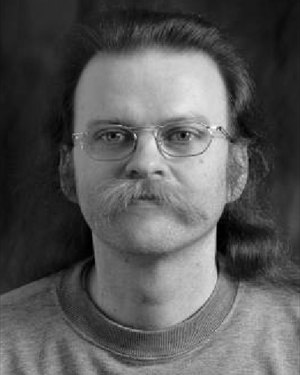 Gerhard Schrom合作论文数Intel Corporation4keith j hodgson合作论文数3Michael Zelikson合作论文数3Tamir Salus合作论文数3
 Nicolas Butzen合作论文数Department of Electrical Engineering, KU Leuven Heverlee3
 Christopher Schaef合作论文数Intel Corporation3
 Takao Oshita合作论文数3
 Vivek De合作论文数Intel3
 Khondker Zakir Ahmed合作论文数Department of Electrical and Electronic Engineering, East West University3
 Praveen Mosalikanti合作论文数3
 Jim Tschanz合作论文数Circuit Research Lab, Intel Corporation3tim abels合作论文数2Rachid Rayess合作论文数2tim gates合作论文数2Mat Manusharow合作论文数2Siddarth Kulasekaran合作论文数2huong t do合作论文数2michael w rogers合作论文数2
 Alex Lyakhov合作论文数Intel IDC Design, Haifa, Israel2
 Fabrice Paillet合作论文数2
 Edward a Burton合作论文数intel2
 Mark Neidengard合作论文数2
 Daniel J. Deleganes合作论文数2
 David Duarte合作论文数2George Geannopoulos合作论文数2Anup Deka合作论文数1Humberto Caballero合作论文数1Carlos Mariscal合作论文数1Rajiv Kaushal合作论文数1William J. Lambert合作论文数1Keng Chen合作论文数1Aruna Payala合作论文数1Shunjiang Xu合作论文数1Ankireddy Nalamalpu合作论文数1
 A V Anil Kumar合作论文数1




