This paper presents a circuit solution for a Radiation-Hardening-by-Design (RHBD) Triple Modular Redundancy (TMR) flip-flop (FF) with self-correction (SC). The baseline TMR is enhanced with additional structures to filter transients and consists of modified latch stages that enable self-correction. Moreover, special spacings are introduced at layout-level to maintain the radiation hardness. The internal states of the triplicated flip-flops are compared and potential bit-flips are detected, internally corrected even though the clock activity has stopped. Thus, the proposed cell supports clock gating (CG) and stores the data reliably as discussed and confirmed by transistor-level simulation results. The novel self-correcting RHBD TMR flip-flop is arranged as a compatible standard cell and is optimized for a low overhead in power, area, and delay which is close to the performance of the standard unhardened counterpart. A prototype chip with special self-correcting test registers is fabricated in a 130 nm BiCMOS technology. As radiation experiments have shown, the proposed RHBD TMR flip-flop is robust up to an LET above 52.5 MeV cm2 mg-1.
Spike-Timing-Dependent Plasticity (STDP) is a biological-plausible learning mechanism widely adopted for building Spiking Neural Networks (SNNs). It determines plasticity polarity and synapse strength change according to the timing difference between pre-and postsynaptic spikes. The learning curves of STDP differ in temporal window size, magnitude and polarity across different synapse types and brain regions and even within a cell, in different dendritic compartments. To accelerate on-chip STDP learning, various implementations have been proposed. However, they either introduce significant latency due to costly counter-based time difference calculation and substantial area cost due to the implementation of weight change LUTs, or lose biologically-plausible timing information due to oversimplification. For low-cost and efficient on-chip learning, a high-throughput Implicit-timing STDP (ImSTDP) with optimized SR depth and a low-cost register-based Implicit-Timing Look-up (ITL) are proposed. ASIC implementation in 22 nm technology demonstrates that ImSTDP can achieve up to 2 $\times$ throughput improvement and 3.61 $\times$ power efficiency improvement at 27% less area cost compared to the cutting-edge counter-LUT on-chip STDP learning solution.
Saving power is one of the most important things in space applications and power consumption has a direct impact on system complexity and costs. One straightforward approach to reduce the power of digital systems is to stop the clock activity, i.e., clock gating (CG). When circuits are exposed to radiation and the clock activity has stopped, resulting upsets accumulate and may destroy the systems' configuration. Thus, a self-correction (SC) mechanism has to be developed in order to mitigate Single Event Effects (SEE) even though the clock signals are deactivated. This paper proposes a circuit solution for self-correcting Radiation-Hardening-by-Design (RHBD) Triple Modular Redundancy (TMR) flip-flops. The transistor- and gate-level schemes are presented, discussed and compared. A prototype chip is fabricated in a 130nm BiCMOS technology. Radiation results show a robustness in LET above 52.5MeVcm(2) mg(-1) for the novel self-correcting RHBD TMR flip-flop.
Clock gating is a common approach for reduction of dynamic power consumption in digital designs. It is achieved by insertion of special clock gating cells in the circuit, enabling to switch off the clock signal to selected flip-flops. However, as the clock gating cell is composed of a latch and a logic gate, it may be affected by the Single Event Upsets (SEUs) and the Single Event Transients (SETs) in radiation environment such as space. Given that a single clock gating cell may be connected to many flip-flops, a fault in one clock gating cell may lead to the circuit or system malfunction. Therefore, solutions for SET and SEU mitigation in clock gating cells are necessary for rad-hard designs. This work introduces two clock gating cell designs based on the use of a delay element and a guard gate to filter input SETs, and triple modular redundancy (TMR) to mitigate SEUs. The TMR concept can also provide enhanced immunity to permanent errors. The proposed designs have been optimized to minimize the number of transistors and improve the SET robustness of internal nodes.
We present a method employing Answer Set Programming in combination with Approximate Model Counting for fast and accurate calculation of error propagation probabilities in digital circuits. By an efficient problem encoding, we achieve an input data format similar to a Verilog netlist so that extensive preprocessing is avoided. By a tight interconnection of our application with the underlying solver, we avoid iterating over fault sites and reduce calls to the solver. Several circuits were analyzed with varying numbers of considered cycles and different degrees of approximation. Our experiments show, that the runtime can be reduced by approximation by a factor of 91, whereas the error compared to the exact result is below 1%.
Single Event Transients (SETs), i.e., voltage glitches induced in combinational logic as a result of the passage of energetic particles, represent an increasingly critical reliability threat for modern complementary metal oxide semiconductor (CMOS) integrated circuits (ICs) employed in space missions. In rad-hard ICs implemented with standard digital cells, special design techniques should be applied to reduce the Soft Error Rate (SER) due to SETs. To this end, it is essential to consider the SET robustness of individual standard cells. Among the wide range of logic cells available in standard cell libraries, the standard delay cells (SDCs) implemented with the skew-sized inverters are exceptionally vulnerable to SETs. Namely, the SET pulses induced in these cells may be hundreds of picoseconds longer than those in other standard cells. In this work, an alternative design of a SDC based on two inverters and two decoupling capacitors is introduced. Electrical simulations have shown that the propagation delay and SET robustness of the proposed delay cell are strongly influenced by the transistor sizes and supply voltage, while the impact of temperature is moderate. The proposed design is more tolerant to SETs than the SDCs with skew-sized inverters, and occupies less area compared to the hardening configurations based on partial and complete duplication. Due to the low transistor count (only six transistors), the proposed delay cell could also be used as a SET filter.
This paper reports our latest implementation results of a fully unrolled LDPC decoder prototyped in 28 nm CMOS technology. The decoder achieves 1218 Gbps coded throughput and consumes a 5.49 mm 2 chip area. The standard min-sum decoding algorithm with four-bit quantization, five unrolled iterations, (648,540) parity matrix, and a seven-stage pipeline is employed. Such implementation achieves a higher data rate than adaptive degeneration and finite-alphabet decoding algorithms, requires less silicon than the solutions mentioned above, and is fully compliant with the IEEE 802.11n WLAN standard.
In this paper, we propose pipelining and unrolling schemes for ultra-high speed belief propagation polar decoders. The proof of concept implementation in 28 nm CMOS technology achieves 1380 Gbps of coded throughput with a short polar codeword length of 512 bits, placing it as one of the fastest soft-decision FEC implementations published so far. With a codeword of length 1024 bits, the decoding throughput can be even higher. Moreover, the decoder shows better error correction performance than other ultra-high speed polar decoders published recently. The consumed chip area is 5.98 mm 2 , and the chip uses five unrolled iterations with constant quantization of four bits at every processing stage.
Instruments for measuring the absorbed dose and dose rate under radiation exposure, known as radiation dosimeters, are indispensable in space missions. They are composed of radiation sensors that generate current or voltage response when exposed to ionizing radiation, and processing electronics for computing the absorbed dose and dose rate. Among a wide range of existing radiation sensors, the Radiation Sensitive Field Effect Transistors (RADFETs) have unique advantages for absorbed dose measurement, and a proven record of successful exploitation in space missions. It has been shown that the RADFETs may be also used for the dose rate monitoring. In that regard, we propose a unique design concept that supports the simultaneous operation of a single RADFET as absorbed dose and dose rate monitor. This enables to reduce the cost of implementation, since the need for other types of radiation sensors can be minimized or eliminated. For processing the RADFET's response we propose a readout system composed of analog signal conditioner (ASC) and a self-adaptive multiprocessing system-on-chip (MPSoC). The soft error rate of MPSoC is monitored in real time with embedded sensors, allowing the autonomous switching between three operating modes (high-performance, de-stress and fault-tolerant), according to the application requirements and radiation conditions.
This work investigates the use of pulse stretching inverters for monitoring the variation of flux and Linear Energy Transfer (LET) of energetic particles. The basic particle detector consists of two cascaded pulse stretching (skew-sized) inverters designed in CMOS technology, and the required sensing area is obtained by connecting multiple two-inverter pulse stretching cells in parallel, and employing the required number of parallel arrays. The particle strikes are detected in terms of the Single Event Transients (SETs), and the detector provides the information on the SET count rate and SET pulse width variation, from which the particle flux and LET can be determined. The main advantage of the proposed solution is the possibility to sense the LET variations using purely digital processing logic. The SPICE simulations done on IHP 130 nm bulk CMOS technology have shown that the SET pulse width at the output of detector changes by 550 ps over the LET range from 1 to 100 MeVcm2mg-1. The proposed solution is intended to operate as an on-chip particle detector within the self-adaptive multiprocessing systems.
In this paper, a solution for tunable filtering of Single Event Transients (SETs) in self-adaptive fault-tolerant systems for space applications is presented. The filter is composed of digitally controlled capacitive delay cells. Each delay cell is made of a MOS capacitor realized with an NMOS transistor, and an NMOS transistor for switching the capacitors. By tuning the filterable SET pulse width, e.g., according to the measured radiation intensity, the power and performance penalties can be controlled online. Electrical simulations on 130 nm bulk CMOS technology have shown that with six active (switched on) delay cells, the SETs shorter than 750 ps can be filtered. The filterable SET pulse width is linearly dependent on the transistor sizes and number of active delay cells. Moreover, the supply voltage, temperature and process variations may significantly affect the filter response, which must be taken into account in the design phase. Based on the simulation results, a predictive model for the filterable SET pulse width as a function of the number of active delay cells, supply voltage and temperature, has been established.
The radiation-induced voltage glitches, known as Single Event Transients (SETs), represent an increasingly critical reliability threat for CMOS integrated circuits (ICs) employed in space missions. In ICs realized with standard digital cells, special design measures are required to reduce the sensitivity to SETs. The standard delay cells implemented with skew-sized inverters are exceptionally vulnerable to SETs, as the SET pulses induced in these cells may be significantly longer than those in other stan-dard cells. In this work, the SET robustness of an alternative design of delay cells based on two inverters and two decoupling capacitors is investigated. Electrical simulations have shown that the SET robustness of the proposed delay cell is inversely related to the propagation delay. With appropriate transistor sizing, the proposed design is more tolerant to SETs than the standard delay cells with skew-sized inverters.
A shortage of practically skilled computer science graduates affects academia as well as the industry. Especially when it comes to hardware design and awareness about the complete digital design flow, a lack of qualified personell can hinder the progess of development teams. To address this issue, we will present the design of an integrated circuit (IC) containing a power- and area optimized neural network, enabling know-how development of the students various key skills required for hardware design. This example project, targeting bachelor and master students interested in hardware engineering and artificial intelligence, offers learning potential in various fields and enough room for creative design decisions and detailed discussions. Possible design options and improvements are discussed throughout the paper with focus on their educational aspects.
Reliability and fault tolerance needs in space applications pose additional requirements to the chip design flow. In order to successfully cope with space related issues, cross-layer measures need to be taken at different levels of design abstraction. In the first place, Single Event Effects (SEEs) need to be well understood and modelled at gate and circuit level. Such evaluation needs to be considered in the process of corresponding rad-hard library design. At cell/gate and RTL levels different methods of redundancy can be applied to accommodate the increased reliability requirements. Since redundancy approaches are very expensive in terms of area, power and performance overhead, effort needs to be spent in optimization. Such optimization could be accomplished through the selective hardening of the most sensitive gates. For example, at gate level the most sensitive combinational cells can be hardened, while at R TL level only critical registers are made fault tolerant. Finally, the design flow could address the highest (system) level of complex digital systems. In this case resilient mechanisms could be implemented, enabling the use of system level redundancy in an adaptive, self-aware and optimal way. In this paper we will propose a rad-hard design flow which supports the evaluation of fault tolerance methods at different abstraction layers.
Answer Set Programming (ASP) is proposed as a compact and versatile approach to circuit analysis. By the example of upsets in registers we demonstrate how to perform reliability analysis in less than 200 lines of code. By an efficient problem encoding we achieve an input data format similar to a Verilog netlist so that extensive preprocessing is avoided. No development of algorithms is required as the analysis relies on elaborate and highly optimized ASP solvers. Exemplary results for a wide range of circuits are presented and potential optimizations are pointed out.
For the time being, ΔΣ ADCs used in the space environment mainly target applications in the LF band. This paper presents a research project that explores a ΔΣ ADC architecture for operation in the MF/HF bands. The SG13RH technology, that offers characterization data under radiation and hardened devices, was selected to implement the test vehicles of this research. Additionally, the suitability of the proposed architecture for a future migration to ultra-deep submicron CMOS nodes is also considered.
Use of a standard non-rad-hard digital cell library in the rad-hard design can be a cost-effective solution for space applications. In this paper we demonstrate how a standard non-rad-hard flip-flop, as one of the most vulnerable digital cells, can be converted into a rad-hard flip-flop without modifying its internal structure. We present five variants of a Triple Modular Redundancy (TMR) flip-flop: baseline TMR flip-flop, latch-based TMR flip-flop, True-Single Phase Clock (TSPC) TMR flip-flop, scannable TMR flip-flop and self-correcting TMR flipflop. For all variants, the multi-bit upsets have been addressed by applying special placement constraints, while the Single Event Transient (SET) mitigation was achieved through the usage of customized SET filters and selection of optimal inverter sizes for the clock and reset trees. The proposed flip-flop variants feature differing performance, thus enabling to choose the optimal solution for every sensitive node in the circuit, according to the predefined design constraints. Several flip-flop designs have been validated on IHP's 130nm BiCMOS process, by irradiation of custom-designed shift registers. It has been shown that the proposed TMR flip-flops are robust to soft errors with a threshold Linear Energy Transfer (LET) from (32.4 MeV.cm(2)/mg) to (62.5 MeV.cm(2)/mg), depending on the variant.
Simulation-based fault injection is an approach, which is usually conducted in the design phase to evaluate the reliability of circuits. However, this approach is frequently time-consuming, especially for large designs. This paper explores the possibilities of applying machine learning (ML) as enhancement to the fault injection to reduce the runtime of the fault verification. The proposed approach separates the target gates for fault injection into two subsets. Standard simulation-based fault injection is only performed for first subset to get the result of fault propagation in the circuit, and enables machine learning process. Based on such partial classical fault injection campaign, a dataset is built to train and validate machine learning models that are able to predict the fault injection result of the remaining gates. The machine learning approach is based on a set of relevant features that could be easily extracted based on the netlist. The dataset in this study, used to validate the approach, is obtained from the ADC digital core. We have evaluated this netlist and provided ML-driven assessment whether the fault injection in some gate will propagate to primary outputs. We have evaluated several machine learning models with different loss functions. The best prediction accuracy is 95% and achieved by a 4 layer neural network with weighted Cross Entropy.
The paper presents an alternative Single-Event Effect (SEE)-tolerant Triple Modular Redundancy (TMR) circuit topology for space applications. The proposed D-flip-flop circuit scheme is fully digitally designed and consists of local Single Event Transient (SET) filter for transient mitigation on the datapath. A latch-based master-slave decomposition with the usage of commercially available unhardened standard cell components is selected. The baseline architecture and the proposed multi-row cell layout is briefly described. Corresponding shift register test vehicles are implemented in 0.13 µm BiCMOS technology. An SEE robustness of a selected candidate with an LET of 46.1 $\frac{\text{MeV} \cdot \text{cm}^{2}}{\text{mg}}$ is measured as a proof of concept.
This paper presents the integration and channel characterization of a highly integrated dual-band digital beamforming space-borne synthetic aperture radar (SAR) receiver. The proposed SAR sensor is a low-cost, lightweight, low-power consumption, and dual-band (X/Ka) dual-polarized module ready for the next-generation space-borne SAR missions. In previous works, by the authors, the design and experimental characterization of each sub-system was already presented and discussed. This work expands upon the previous characterization by providing an exhaustive experimental assessment of the fully integrated system. As it will be shown, the proposed tests were used to validate all the instrument channels in a set-up where the SAR sensor was illuminated by an external source minim the ground reflected waves. Test results demonstrate how the system channels are properly operating allowing the reception of the input signals and their processing in the digital domain. The possibility to easily implement a calibration procedure has also been validated to equalize, in the digital domain, the unavoidable amplitude differences between the different channels.
 Milos Krstic合作论文数IHP46
 Marko S. Andjelkovic合作论文数Faculty of Electronic Engineering, University of Niš19
 Anselm Breitenreiter合作论文数IHP, Technol Pk 25, Frankfurt, Oder, Germany18
 Steffen Zeidler合作论文数10
 Aleksandar Simevski合作论文数7
 Junchao Chen合作论文数5
 Chunxu Mao合作论文数University of Surrey5
 Tobias Rommel合作论文数German Aerosp. Center (DLR),, Microwave & Radar Inst.;c;German Aerosp. Center (DLR),, Microwave & Radar Inst.5
 Steven Gao合作论文数School of Engineering, University of Kent5
 Marwan Younis合作论文数Institute of Radio Frequency Engineering and Electronics, Karlsruhe Institute of Technology;Microwaves and Radar Institute, German Aerospace Center5
 Goran Panic合作论文数5
 Luigi Boccia合作论文数Dipartimento di Elettronica, Informatica e Sistemistica Via Bucci, Università della Calabria5
 Giandomenico Amendola合作论文数Dipartimento di Elettronica, Informatica e Sistemistica Via Bucci, Università della Calabria5
 Srdjan Glisic合作论文数5
 Emilio Arnieri合作论文数University of Calabria5klaus tittelbachhelmrich合作论文数4Grass, E.合作论文数4
 Rolf Kraemer合作论文数4
 Frank Winkler合作论文数Department of Physics, Middlebury College4
 Piotr Penkala合作论文数4
 Zoran Stamenkovic合作论文数3
 Alexey Balashov合作论文数3
 Stefan Ilic合作论文数3
 Uroschanit Yodprasit合作论文数3
 Frank Herzel合作论文数3
 Xin Fan (樊鑫)合作论文数International School of Information Science and Engineering, Dalian University of Technology - Ritsumeikan University3
 Carlos Benito合作论文数Department of Neuroradiology, Hospital Gregorio Marañón3
 Marisa Lopez-Vallejo合作论文数Universidad Politécnica de Madrid3Frank Vater合作论文数3
 Felipe A. Kuentzer合作论文数Department of Informatics, University of Santa Cruz do Sul3Ulrich a Jagdhold合作论文数3
 Goran S. Ristic合作论文数Department of Microelectronics, Faculty of Electronic Engineering, University of Niš;Applied Physics Laboratory, Faculty of Electronic Engineering, University of Niš3A. Hasani合作论文数2A. Loose合作论文数2P. Penkala合作论文数2
 Alberto J Palma合作论文数2
 Pedro Reviriego合作论文数2arkadiusz koczor合作论文数2
 Jesus Gutierrez合作论文数IHP Leibniz-Institut;r innovative Mikroelektronik2Markus Appel合作论文数2
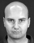 Vladimir Petrovic合作论文数2
 Mahdi Tala合作论文数2
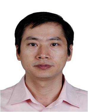 Yuanqing Li (李远清)合作论文数Center for Brain Computer Interfaces and Brain Information Processing, School of Automation Science and Engineering, South China University of Technology;Panzhou Lab2
 Gunter Fischer合作论文数2
 Dietmar Kissinger合作论文数Institut für Elektronische Bauelemente und Schaltungen, Universitat Ulm2
 Antonio M. Lallena合作论文数Departamento de F ´ õsica Moderna;Universidad de Granada;Departamento de F ´ õsica Moderna, Universidad de Granada2
 Nebojsa Maletic合作论文数2
 Aleksandar B. Jaksic合作论文数2
 Lukasz Lopacinski合作论文数2




