The objective of this paper is to present the design of a high-power amplifier using the Wilkinson power divider/combiner methodology. The single-stage power amplifier is based on a GaN HEMT transistor and operates in class AB. By employing the Wilkinson-based power combining approach, the output power was successfully increased from 45 dBm (for the single-stage amplifier) to 48.827 dBm at 3 GHz. In addition to the enhanced output power, the achieved gain of 15 dB and efficiency of 65% demonstrate high performance compared to previous works. Designed using microstrip technology, the resulting power amplifier is well-suited for S-band applications such as wireless and satellite communications, as well as Radar systems.
This paper outlines the development of an S-band Power Amplifier (PA) with a GaN HEMT technology transistor to achieve high output power. The methodology used in this study is the loadpull technique, which aims to determine the optimal impedance for maximizing gain and efficiency. The matching process involved the use of impedance transforming lines in microstrip technology. The design of the PA matching networks incorporated two impedance transforming lines. Their characteristics parameters were calculated before moving to simulations on ADS software (Advanced Design System). Through the use of an optimization tool, a successful matching was achieved. The resulting device demonstrated an output power of 42.532 dBm, a maximum gain of 13.532 dB, and a Power-Added Efficiency (PAE) of 56.501%.
Nowadays, there is a panel of radio-frequency Power Amplifiers (PA) designed with various techniques and for different applications as they are required to amplify a signal. This paper presents the design of a Power Amplifier, based on a GaN HEMT transistor, that can operates in class AB and at an S-band frequency of 3 GHz. This frequency is suitable for weather radar applications. GaN technology is on the rise due to its properties, such as its ability to work at high frequencies. The proposed Power Amplifier matching networks were designed with microstrip lines by using a simple impedance transforming line, whose characteristics were calculated before simulations on ADS (Advanced Design System) and achieve a good matching. The fabricated device reached an output power of 41.23 dBm, and a maximum gain of 11.76 dB.
Electronic devices with high performances like Power Amplifiers (PA) are very important for Wireless communications. This paper proposes a design of a class AB power amplifier operating at 2.45 GHz, in the S-band frequency. The Cree's CG2H40045F GaN HEMT (High Electron Mobility Transistor) is used for this design. The Gallium Nitride (GaN) technology has been chosen in light of its advantageous properties such as high breakdown voltage, high band gap, as well as high thermal conditions. The paper investigates the different design trade-offs for finding a good balance between various key parameters of the PA (linearity, efficiency, and gain). A design approach has been proposed and the microstrip lines based on the Smith Chart tool available in ADS software have been used for the matching process. The class AB was selected to reach a good agreement between linearity and efficiency, provided by this class. After various process applications from DC characterization to simulations, the proposed design achieves a power added efficiency more than 50% at power saturation with a gain of 15 dB in schematic simulation. The layout dimensions are 55.5 × 64.45 mm 2 on PCB technology.
The Gallium Nitride GaN based power switching device EPC2206 has a Land Grid Array (LGA) packaging with a pitch between pads of 400 mu m. This low pitch does not facilitate transistor connection on a test vehicle in the context of aging tests where the component must undergo repetitive sequences of I(V) and C(V) characteriza-tions, threshold voltage, leakage currents and then repetitive stress. Thus, the purpose of this paper is to adapt this encapsulated power switching device for coaxial or coplanar type measurements and to look for the best configuration to move this transistor from one test bench to another by using an adaptation system on a printed circuit board (PCB). To choose the best performances of three adaptation system configurations, this paper presents, on the one hand, an experimental study on I(V) characterization, threshold voltage Vth, drain leakage current Idss, gate leakage current Igss. On the other hand, a series of measurements of these different charac-teristics was carried out on the three EPC2206 connection configurations to validate the reproducibility of the measurements.
Due to the superior physical properties of Wide bandgap (WBG) based power switching devices, silicon carbide (SiC) and gallium nitride (GaN) are believed to be promising candidates to replace Silicon in power electronics converters for EV/HEV applications. That is for this reason that the reliability of these switching devices is an important parameter which conditions their insertion in industrial applications. It is in this context that the subject of this paper falls, aiming at studying the reliability of these new generations of transistors by implementing an in-situ monitoring system in a 48 V/12 V DC/DC converter in order to monitor the evolution of the Rdson. Therefore, we propose a study focusing in the monitoring of Rdson considered as one of more important degradation indicator of a GaN transistor. After an introduction presenting the context of the study, the principle of PHM is described in this paper. The GaN transistor and its use in DC/DC converters are described. The method for monitoring Rdson, a sensitive parameter of the transistor, is developed. The simulations highlight the interest of such a monitoring method to predict the ageing of the transistor, while emphasising the practical difficulties of implementation.
This paper presents a complete methodology based on an accurate S-parameters calibration procedure to determine parasitic resistances, inductances, and capacitances of a packaged GaN power transistor. Results show the possibility to extract very low device parasitics which may influence switching mechanisms in power converters. The accuracy of the S parameter characterization is verified on a SiC power MOSFET. Good agreement is found between extracted values and technical data provided in the literature. The extracted linear model of the tested GaN HEMT is simulated in the frequency domain using an S-parameters circuit simulator. The excellent match between the measurement and simulation indicates a high accuracy of the S-parameter extraction technique. The GaN HEMT parasitic elements are obtained from the S-parameters measured using a vector network analyzer and then converted to the impedance (Z) parameters. These parameters, through detailed network analysis, provide more accurate values of the internal parasitic inductances than the commonly used LCR meter measurement technique. The method has the capability to be applied to any packaged GaN power transistor fabricated by different manufacturers.
The quality of the gate-oxide and Oxide/SiC interfaces is one of the crucial issues in the implementation of silicon carbide (SiC) Metal Oxide Semiconductor Field Effect Transistors (MOSFETs) in the industrial power electronic applications. The main goal of this work is to investigate the gate-oxide integrity and to understand the basic phenomena involved on 4H-SiC MOSFET by the mean of Capacitance-Voltage (C-V) characterizations. The paper presents HTRB (High Temperature Reverse Bias) test results on the second and third generations of SiC MOSFETs. The C-V measurements are compared to physical simulation results. The good agreement between 2D numerical simulations and measurements suggests failures related to acceptor interface traps and doping concentration variations.
An experimental study based on pulsed I-V characterization is conducted at various temperatures to estimate the losses of GaN High-Electron-Mobility Transistors (HEMTs) for switching circuit applications. The estimation of the GaN HEMT power losses is performed by a SPICE simulation using a non-segmented Electro-thermal model. The parameters of this model are extracted using Levenberg–Marquardt Algorithm. The proposed modeling methodology is compared to literature and shows good convergence of static characteristics. The temperature dependency of device parameters is also taken into consideration. Furthermore, the modelled device is verified in a real switching application using a developed efficient switching bench. The verification of the GaN HEMT model shows a good convergence to measurements in term of conduction power losses. Finally, the evolution of the GaN HEMT power losses in switching applications is modelled as a function of the temperature and output current.
In this study, the authors aim at investigating the static electro-thermal behaviour of two new generations of power silicon carbide metal oxide semiconductor field effect transistors (SiC MOSFETs). The studied devices are commercialised and have a vertical structure. Two approaches are followed: device modelling and physical simulation. An improved compact model based on an accurate method of parameters extraction is introduced. The simulation results obtained with this method perfectly fit the measurements. The parameters extracted precisely from the model (threshold voltage, saturation region transconductance and transverse electric field parameter) are used to accurately analyse the static behaviour of 1200 V Gen 2 and 900 V Gen 3 SiC MOSFETs. Physical simulation is conducted to understand the impact of the temperature and the physical parameters on the threshold voltage and the on-state resistance.
this paper presents experimental short-circuit aging tests of a 600V GaN (Gallium nitrite) GIT (Gate Injection Transistor). The short circuit aging tests effect under the drain voltage equal to 35V and the three short-circuit durations (1ms, 2ms and 4ms) are investigated. The evolution of the electrical characterizations is well shown in this paper. A microscopic analysis, related the degradation mechanism, is proposed in the paper.
Threshold voltage (\(V_{th}\)) is one of the most important electrical parameters in silicon carbide (SiC) metal-oxide-semiconductor field-effect transistors (MOSFETs) design, characterization, modeling, and simulation. The reduction of the threshold voltage increases the performance in terms of switching time for the power converter. The study of the evolution of \(V_{th}\) over time must be considered by the designers of the new generations of energy conversion systems. There are several existing methods for \(V_{th}\) extraction, and the aim of this chapter is to compare the commonly used MOSFET threshold voltage extraction methods and to propose a new method based on a physical approach. The extraction method proposed in this chapter is based on the static I–V measurements and the use of the Levenberg–Marquardt optimization algorithm. The implementation of the several extraction methods is tested and discussed by applying them to commercial components in order to evaluate their performance and validity in both the linear and saturation regions. The study is carried out for two generations of power SiC-MOSFETs of CREE constructor.
This paper proposes a methodology to study the reliability and failure analysis of new technologies of power transistors. The use of wide gap materials such as Silicon Carbide (SiC) and Gallium Nitride (GaN) is now a good alternative to meet the integration requirements of energy conversion systems.
This chapter presents the results of a study in which the temperature and the microdisplacements of the chip surface of high-frequency power electronic components used in radar and telecommunication systems are measured. Several techniques are applied. Their advantages, disadvantages and shared fields of application are discussed. Results from several samples show that the different approaches converge. The originality of this study is that the measurements of chip surface temperature and displacement are obtained simultaneously. This approach makes it possible to then calculate the thermal resistance of an electronic component and characterize the evolution of this resistance over component lifetime.
This paper proposes an experimental study of temperature effects on Gallium Nitride (GaN) High Electron Mobility Transistors (HEMTs).The output and transfer characteristics are monitored at temperatures ranging from 5°C to 105°C.The temperature dependency on static parameters of GaN HEMT is examined, such as: drain current (IDS), on-state resistance (RDS(ON)), transconductance (gm), threshold voltage (VTH) and the gate leakage current (IGSS).The decreases of IDS and gm accompanied with the increase of RDS(ON) and IGSS when increasing temperature have been observed.Moreover, the decrease in electron mobility with increasing temperatures is considered to be one of the causes of the reduction in the drain current and transconductance.In order to study the impact of temperature on power converters with GaN HEMTs by simulation approach, the thermal characteristics of a 650V, 30A GaN HEMT have been modelled.The used model is a nonsegmented Electro-thermal SPICE model of Motorola.The model parameters are extracted using Levenberg-Marquardt Algorithm.
This paper investigates the aging of a 650 V, 30 A GaN HEMT power transistor under operational switching conditions. The switching stress respects the Safe Operation Area (SOA) of the tested transistor. The aging campaign lasted 1008 h and was carried out through a developed switching application with high power efficiency. The global aging results show the degradation of five parameters: drain current ID, on-state resistance R-DS(ON), transconductance g(m), gate leakage current I-GSS, and threshold voltage V-TH. The major causes that affect the reliability of the GaN HEMT are hard switching, long time of test and high intensity of the stress. The existence of trapped charge in the gate-drain access region after aging is demonstrated using pulsed measurements. The effects of this degradation on power converters are studied by modeling the static characteristics of the aged GaN HEMT using an accurate method based on the Levenberg-Marquardt Algorithm. The accuracy and consistent convergence of the developed SPICE model provide a good way to investigate the reliability of GaN HEMTs by a simulation approach.
This letter proposes an accurate parameter extraction method based on the Levenberg-Marquardt algorithm for a silicon carbide (SiC) power mosfet model. An improved compact model uses this method to study the static behavior of SiC power mosfets according to the temperature and the input voltage. The simulation results obtained with this proposed method fit perfectly the measurements and accurately describe the static behavior of 1200 V Gen 2 SiC mosfets. The extracted model parameters (threshold voltage, saturation region transconductance, and transverse electric field parameter) are evaluated to analyze the temperature impact and understand the physical behavior of 1200 V Gen 2 SiC power mosfet.
 Olivier Latry合作论文数37
 Eric Joubert合作论文数19
 Ahmed El Oualkadi合作论文数Department of Electrical Engineering, Université Catholique de Louvain19
 F. Fouquet合作论文数11
 Moncef Kadi合作论文数10
 Hichame Maanane合作论文数10
 Mohamed Masmoudi合作论文数Electronics Micro Technology and Communication (EMC) Research Group, Tunisia10M. Ketata合作论文数8Wadia Jouha合作论文数UPS, University of Toulouse8
 Philippe Eudeline合作论文数8Christian Gautier合作论文数7E. Joubert合作论文数7Malika Khettab合作论文数6Ludovic Lacheze合作论文数6
 Philippe Pougnet合作论文数6
 Pierre Richard Dahoo合作论文数Laboratoire de Spectronomie Moléculaire-CNRS 06.0136, Université Pierre et Marie Curie6Hubert Polaert合作论文数6
 Dan Borza合作论文数5patrick martin合作论文数5alain kamdel合作论文数5Al Mehdi Bouchour合作论文数5Jorge Linares合作论文数5Bouchaib Radi合作论文数5
 Philippe Descamps合作论文数5
 Ramanujan, A.合作论文数5Nistea Ioana合作论文数Diamond Light Source, Harwell Science and Innovation Campus5
 Zouheir Riah合作论文数5
 Abdelkhalak El Hami合作论文数LOFIMS-INSA5S. Khemiri合作论文数5Maxime Fontaine合作论文数4
 M. Kadi合作论文数4
 F. Temcamani合作论文数4F.-J. Baylé合作论文数4
 Jean Baptiste Fonder合作论文数3karine dehaismourgues合作论文数3
 Sanae Taoufik合作论文数3
 Jian Zhi Fu合作论文数3
 Cedric Duperrier合作论文数3
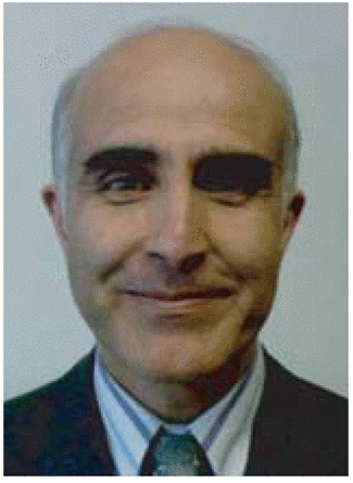 Mohamed Ketata合作论文数3J. P. Sipma合作论文数2S. Mbarek合作论文数2
 Andres Echeverri合作论文数2Fabien Cuvilly合作论文数2
 Shawki Douzi合作论文数2
 Rabii El Maani合作论文数2
 JAMAL ZBITOU合作论文数2
 Farid Temcamani合作论文数2Ph. Eudeline合作论文数2armelle girard合作论文数1




