Approximate computing has garnered significant attention due to its potential to reduce power consumption, enhance performance, and simplify circuit design. However, the security implications of applying approximate computing techniques remain largely unexplored. Identifying all possible vulnerabilities in approximate designs is very challenging. One of the challenges stems from the lack of insightful methodologies and metrics to perform a precise security evaluation. This paper presents ApproPower, a security-driven framework for pre-silicon evaluation of power side-channel leakage in approximate multipliers. ApproPower enables an analysis of how approximation techniques influence power side-channel leakage and employs symbolic path analysis to estimate delay-dependent power leakage behaviors at design time. Using a set of open-source approximate multipliers, we examine the relationship between data precision, approximate strategies, and measured power leakage. Our results show that symbolic path analysis provides useful guidance for identifying potential power side-channel risks. We also observe that some approximate designs can offer improved resource efficiency while exhibiting reduced leakage; for instance, in the mul7x7u set, a majority of benchmark circuits demonstrate lower leakage after approximation, with mul7x7u_03M achieving a 35% reduction in resource usage compared to mul8x7u_3C6.
This work presents a programmable processor for both neural-network (NN)-based inference and localization in micro-robotic visual perception (VP). While specialized accelerators for the two applications demonstrate substantial energy efficiency and throughput gains, the built-in system with separate cores suffers from a mismatch across diverse robotic tasks, making it difficult to harness energy- and area-efficiency gains at the system level, which are the two critical metrics for intelligent computing platforms on micro and even more miniaturized robots, such as robot insects. To overcome this limitation, we employ a unified VP architecture that features a reconfigurable spatial array to perform matrix multiplication and decomposition, along with further fusion of different key operators from circuit level to architecture level, including a hybrid precision dataflow and a customized ISA. This leads to a unified processor for programmable computation across the micro-robotic VP domain, enabling: 1) efficient acceleration for both localization and NN inference; 2) flexible mapping of diverse tasks to the accelerator. Fabricated in 28 nm, the prototype achieves a peak area efficiency of 62.2 fps/mm(2) and a peak energy efficiency of 116 uJ/frame when performing visual navigation under the energy-efficient mode at 0.6 V, with less than 0.3% accuracy loss compared to full-precision localization running on a commercial CPU. Validated across four typical micro-robotic applications, the prototype demonstrates 8.6 & times; system-level area efficiency compared to a combination of renowned NN inference and localization accelerators.
Generative large language models (LLMs) in cloud services impose substantial memory demands due to massive parameters and large key-value caches, especially in long-context scenarios. To overcome bandwidth and capacity limits of conventional memory systems, hybrid memory and 3D-stacked architectures have emerged as promising solutions. However, prior Non-Volatile Memory (NVM)-DRAM hybrid architecture studies often characterize NVM as dense but bandwidth-limited storage, overlooking its potential for favorable bandwidth-capacity tradeoffs enabled by the areal bandwidth scaling in true 3D stacking. To tackle this problem, our work jointly considers memory and LLM data heterogeneity to reveal opportunities at the workload-hardware interface. Guided by this characterization, we propose SHyLA, a hardware-software heterogeneity-aware 3D-stacked NVM-DRAM hybrid architecture for LLM inference. SHyLA strategically places different LLM data categories across memory devices and employs a bandwidth-utilization-centric dataflow that exploits the areal bandwidth of 3D stacking, particularly under hybrid memory data placement constraints. A two-stage design space exploration methodology further navigates the expanded hybrid memory and deployment design space to maximize system throughput under per-user throughput constraints with architectural insights. Evaluations demonstrate that SHyLA achieves up to $5.84 \times (\mathbf{2. 0 2} \times$ geomean) over a DRAM-only baseline and up to $\mathbf{6. 0 3} \times$ (1.76× geomean) over an NVM-only baseline, while maintaining acceptable thermal behavior and a practical lifetime.
AI and HPC infrastructure increasingly serves workload portfolios that combine dense tensor computation, sparse kernels, large memory footprints, and communication-intensive collectives. Supporting these portfolios requires coordinated choices across accelerators, memory tiers, scale-up fabrics, and cluster networks. The resulting Cross-layer Heterogeneous System (XHS) design space is difficult to explore: hardware choices change legal task mappings, while rack power, switch radix, cabling, and cost constraints invalidate many candidates. We present CHASE, an application-driven framework that searches physically feasible XHS architectures through the workloads they must execute. CHASE represents candidates as hierarchical typed graphs and rejects designs that violate deployment constraints. It avoids intractable joint hardware-mapping search with a decoupled two-level loop: an inner mapper translates hardware-independent workload DAGs into topology-aware event traces, a calibrated event-driven simulator evaluates each mapping, and an outer telemetry-guided optimizer evolves the hardware graph. We evaluate CHASE on sparse-computing and LLM workloads. Its mapper remains within 6.06% of exhaustive optima while reducing mapping time by 60.5% on average relative to PEFT. Compute-model errors average 4.4-7.5%, and communication validation reproduces key trends across physical platforms. The outer search reaches near-global optima within 64 iterations. End-to-end case studies show that sparse workloads favor criticality-aware heterogeneous pods, whereas LLM inference favors scale-up islands; the resulting designs deliver 6.20$\times$ and 2.12$\times$ geomean speedups, respectively, while reducing cost and power relative to the baselines.
Transformer-based neural networks are pivotal to emerging vision and natural language processing tasks. Despite their success, accelerating these models remains challenging due to their immense computational and memory requirements. Traditional methods, such as sparse attention computing, alleviate some of these burdens but fall short in addressing the complexity of diverse operators and the significant storage overhead caused by large model parameters and low data reuse rates. In this work, we propose BVDT, an energy-efficient Transformer accelerator that exploits inherent matrix redundancy to overcome these limitations through four key innovations. First, BVDT introduces a novel basis-vector decomposition technique that compresses model size by over 25x, supported by unified memory management. Then, it incorporates a dual array core architecture, powered by LUT-assisted computing, featuring an optimized lookup code fetch and LUT programming mechanism. In addition, BVDT employs a block-wise post-fusion mapping method that seamlessly links the compression pattern and computing architecture. Finally, BVDT utilizes a private-to-private highway data-path for multi-core systems, enabling a LUT stationary dataflow that significantly reduces the memory access overhead. Consequently, BVDT provides a task-agnostic optimization across diverse Transformer operators under various workloads. Fabricated in 28-nm CMOS technology, the accelerator achieves an exceptional area efficiency of 4.35 similar to TOPS/mm(2), a 5.1x improvement over prior state-of-the-art solutions. Moreover, BVDT also achieves 1.4x to 3.6x regarding energy efficiency, offering a promising solution for Transformer-based applications.
Computing-in-memory (CIM) is a promising paradigm for energy- and area-efficient implementation of the heavy general matrix multiplication (GEMM) operations, especially in the evolving deep learning algorithms. Though existing CIM macros have demonstrated remarkable energy/area efficiency, the corresponding metrics of the system-level CIM chips degrade due to the peripheral components, including external SRAM and accumulation circuits. First, the separated design of CIM macros and peripheral components leads to suboptimal solutions, suffering high input/output SRAM access power, loose layout with long data paths, bulk clock trees, and so on. Second, the input/output SRAM takes a majority area proportion, which is inevitable in existing system-level CIM chips. Besides, continuous power/area optimization on the CIM macro itself also contributes to the system-level energy/area efficiency. Third, the accumulation module after the CIM macro leads to redundant power consumption due to the unnecessary high-bit-position computation. This work presents a system-in-one-macro CIM chip, integrating all system-level components (except the control logic) into one single macro, indicating a significant difference in the design flow with three detailed innovations: 1) to replace the power/area consuming external SRAMs, a high-density leakage-eliminated 2T1C embedded DRAM (eDRAM) is designed for input activation and output result storage; 2) a capacitor (cap)-over-logic one-transistor-one-capacitor (1T1C) eDRAM array with shared-preprocessing MUX-based CIM circuits is proposed to further improve the macro-level CIM energy/area efficiency and density; and 3) utilizing the low-activity property of the high-bit-position accumulation, a low-MAC-aware near-memory-computing (NMC) circuit is designed to reduce the redundant accumulation power. The 28-nm fabricated system-in-one-macro CIM chip demonstrates 51.6 TOPS/W energy efficiency, 1.53 TOPS/mm2 area efficiency, and 2.22-Mb/mm2 storage density.
Dynamic memristors (DMs) coupled with Geiger-mode avalanche photodiodes (GmAPDs) break through the resistor capacitor (RC) constraints of passive quenching, yet demand integration to realize miniaturization and scalable fabrication, which is challenged by the penetration of active metal ions of DM into GmAPD's semiconductor materials. This work introduces a practical method to tackle the issue through a dense alumina barrier layer deposition and a meticulously designed DM electrode arrangement. As a result, the dark current of GmAPD is decreased by an order of magnitude, and GmAPD resumes its reliable avalanche pulse response. The recovery time is reduced from microseconds to tens of nanoseconds (30 & times; improvement) compared to fixed resistor quenching. The detector achieves a 10-fold improvement in counting rate at a frequency of 25 MHz. This architecture paves the way for scalable silicon photomultipliers (SiPMs) with enhanced sensitivity and timing resolution, critical for LiDAR and quantum communication.
Point cloud data are widely utilized in autonomous driving and embedded intelligence; however, their inherently large yet highly sparse nature imposes significant challenges on conventional GPU architectures due to low computational and memory efficiency. This paper presents an algorithm-hardware co-optimization framework to enhance deployment efficiency on resource-constrained edge devices. First, a lightweight semantic-aware network is developed to remove more than 90% of redundant background points while maintaining detection accuracy with minimal degradation. Second, an adaptive octree-based partitioning scheme is introduced as a hardware-aware preprocessing step, effectively minimizing memory and computation overhead under resource constraints. Experiments on the KITTI dataset with the SECOND 3D backbone demonstrate up to 36.98× computational speedup and 35.68× memory access speedup over the baseline, with only a 3.6% reduction in 3D AP for the Car category. These results validate the proposed framework’s effectiveness in enabling efficient and real-time point cloud perception on edge devices.
Recent quantized neural networks require various dynamic ranges and resolutions to enable better inference accuracy, necessitating mixed support of energy-efficient integer and floating point computation. This work presents an SRAM look-up table (LUT) based INT8/FP8 dual mode in-memory-computing (IMC) macro which supports configurable FP8 (E4M3 and E5M2) multiply-accumulate (MAC) operation and 2:8 structural sparsity pruning. Instead of suffering either excessive overheads of shifting and alignment logic or accuracy degradation for extreme energy efficiency, this macro exploits fine-grain exponent sharing and efficient LUT-based MAC circuits to balance the two aspects. The key features are: (1) a pipelined and SNR-oriented mantissa and exponent execution circuit for FP8 multiplication; (2) a LUT-based shifter and 1-stage adder to reduce digital logic overhead in FP MAC; (3) an in-macro decoder to support 2:8 structural sparsity pruning. The silicon prototype in 28nm CMOS achieves 81.69% accuracy for DeiT-base model for ImageNet dataset in dense FP8 mode, and 76.15% accuracy for ResNet-34 model in CIFAR100 dataset in sparse FP8 mode. The 2:8 pruning provides a 31.42 TFLOPS/W peak energy efficiency and 3.56 TFLOPS/mm2 peak area efficiency in sparse FP8 mode.
Tiny machine learning (tinyML) brings machine intelligence to numerous extreme edge scenarios under battery-powered and always-on constraints, which imposes demands on tinyML processors for ultra-low power and versatile support for diverse applications and tinyML models. A heterogeneous-computing-fabric (hetero-fabric) architecture that incorporates compute-in-memory (CIM) core and multiply-accumulate (MAC) unit-based digital core (Dcore) can combine high energy efficiency and flexibility to meet such demands. However, the dataflow flexibility in the hetero-fabric architectures has not been well explored. Besides, previous CIM macros are limited by the inherently fixed compute-storage ratio, facing the dilemma of balancing compute and storage density requirements from shallow to deep layers in neural network models. This work presents a versatile tinyML SoC for diverse extreme edge ML tasks. Firstly, we propose a tightly-coupled hetero-fabric architecture for tinyML processing, where the CIM core (Ccore) and Dcore are tightly coupled through the reconfigurable data-streaming network (RDSN). Flexible inter-/intra-core dataflow orchestration for various tinyML models with reduced L1 memory access is further proposed. We also propose a layer-wise dynamic frequency scaling (DFS) scheme for hetero-fabric performance balance with adjustable inter-core clock frequency ratios. Further energy savings can be achieved when combined with dynamic voltage scaling (DVS). Besides, we propose a three-mode reconfigurable-LUT (R-LUT) CIM macro, which breaks the inherent compute-storage limitations and enables dynamically adjustable compute and storage density. A compact Twin-10T SRAM cell featuring lower read power is also proposed to construct the LUT array. Finally, we design a flexible Dcore featuring intra-core fine-grained workload partition and elaborate scheduling to coordinate with the Ccore for dataflow orchestration. The fabricated 28nm chip achieves $2.14\times $ higher SoC energy efficiency than state-of-the-art CIM-based tinyML SoC. It supports all MLPerf Tiny tasks, achieving practical performance (e.g., no less than 30 fps) with no more than 0.5mW power.
A modeling/rendering unified 3D GS processor is proposed with: 1) A locality-aware dynamic fine-grained rendering engine for reduced redundant computation. 2) A locality-optimized unified rendering workflow to reduce EMA. 3) A unified reconfigurable architecture for neural modeling and Gaussian rendering with minimal area overhead. It achieves $3.4 \times$ higher rendering throughput and 74.1% lower energy per frame than SOTA 3D GS accelerators, and an orders-of-magnitude reduction in modeling latency.
Diffusion Policy (DP) has demonstrated strong potential in robotic visuomotor control, offering robust generalization and seamless integration of multi-modal data. However, its complex model structure and increasing multi-modal inputs have brought latency and power challenges for edge resource-constrained robotic platforms. To address the above challenges, we identify the potential intra-model and inter-model redundancies in DP. We observe that DP relies on frequent multi-modal inputs such as images and text during execution. However, the demands of fine-grained robotic manipulation result in substantial intra-modal similarity across consecutive image frames, which, combined with inter-modal semantic redundancy between images and language, indicates that much of the input information is repetitive and potentially compressible. Yet prior works have not exploited these characteristics for targeted optimization. We therefore propose a hardware–software co-design accelerator. On the algorithmic side, we introduce self- and cross-guided modal compression, leveraging intra- and inter-modality similarity to reduce redundant computation within the key DP modules. On the hardware side, we design a tailored architecture that supports multiple operators with optimized sparse memory access, lightweight computation engines, and reconfigurable on-chip dataflow, substantially reducing energy cost. Experimental results demonstrate a 26× speedup over a high-performance GPU while consuming only 1.5 W, enabling low-power and real-time robotic control on edge robotic devices.
Computing-in-Memory (CIM) is a promising solution for Deep Neural Network (DNN) accelerators, improving performance and energy efficiency by addressing the “memory wall” challenge. Recent Look-Up Table (LUT)-based CIM and Cache-based CIM architectures leverage weight-stationary dataflow and feature-map data locality for energy efficiency. However, applying existing Cache-CIM to high bit-width computation faces two main challenges:(1) High Bit-Width Data Incompatibility: Directly processing high bit-width inputs (e.g., INT12, FP16) lowers cache hit rates and energy efficiency. Maintaining hit rates would require an exponential, and thus prohibitive, increase in cache lines. Bit-serial approaches are also inefficient due to poor data locality in LSBs. (2) Cache-Unfriendly FloatingPoint Alignment: Essential floating-point alignment operations inherently degrade data locality or prevent resource sharing across output channels. To overcome these, we propose Hy2S-CIM, featuring three key contributions: (1) A Hybrid-Cache-LUT CIM architecture that efficiently handles high bit-width computations by decoupling the multiplication of MSBs and LSBs to MSB Cache-based and LSB LUT-based multipliers, respectively. (2) A Cache-Friendly 2-Stage Alignment Scheme that preserves data locality and enables controller sharing. (3) An Area-efficient LUT multiplier that achieves a better tradeoff between the overhead of LUT and decoder. Experiment results show that Hy2S-CIM achieves 1.4x-2.4x energy efficiency improvement over prior CIM architectures on typical vision AI tasks.
This letter presents a switched-capacitor SRAM compute-in-memory macro optimized for TinyML inference. Key features include: 1) an area-efficient folded-differential multiply-and-accumulate (FD-MAC) scheme to double the signal margin; 2) a closed-loop floating-inverter amplifier (FIA)-based charge accumulation technique for signal-to-noise ratio enhancement and multiply-and-accumulate (MAC) voltage integration; and 3) a sparsity-aware multistep MAC method to reduce A/D conversions and improve utilization. Fabricated in a 28-nm process, the 32-kb prototype achieves 68.7 TOPS/W energy efficiency and 1.74 TOPS/mm(2) area efficiency in 8-bit mode.
Computing and communication satellite (CCS) constellation resource scheduling is crucial for efficient onboard processing of remote sensing data. In this letter, we innovatively propose a constraint-aware scheduling (CAS) algorithm for fast resource scheduling of CCS constellation. CAS utilizes the perception of constraint violations in the elite solution at each iteration, specifically for connectivity and memory constraints, to heuristically clear and refill subtask assignments, thereby exploring the solution space efficiently. Experimental results show that the proposed CAS algorithm reduces the runtime of CCS constellation resource scheduling while maintaining the solution quality in comparison with existing state-of-the-art algorithms.
Neural network (NN) accelerators with multi-chip-module (MCM) architectures enable integration of massive computation capability; however, they face challenges of computing resource underutilization and off-chip communication overheads. Traditional parallelization schemes for NN inference on MCM architectures, such as intra-layer parallelism and inter-layer pipelining, show incompetency in breaking through both challenges, limiting the scalability of MCM architectures. We observed that existing works typically deploy layers separately rather than considering them jointly. This underexploited dimension leads to compromises between system computation and communication, thus hindering optimal utilization, especially as hardware/software scale. To address this limitation, we propose Scope, a merged pipeline framework incorporating this overlooked multi-layer dimension, thereby achieving improved throughput and scalability by relaxing tradeoffs between computation, communication and memory costs. This new dimension, however, adds to the complexity of design space exploration (DSE). To tackle this, we develop a series of search algorithms that achieves exponential-to-linear complexity reduction, while identifying solutions that rank in the top 0.05% of performance. Experiments show that Scope achieves up to 1.73x throughput improvement while maintaining similar energy consumption for ResNet-152 inference compared to state-of-the-art approaches.
A modeling/rendering unified 3D GS processor is proposed with: 1) A locality-aware dynamic fine-grained rendering engine for reduced redundant computation. 2) A locality-optimized unified rendering workflow to reduce EMA. 3) A unified reconfigurable architecture for neural modeling and Gaussian rendering with minimal area overhead. It achieves 3.4x higher rendering throughput and 74.1% lower energy per frame than SOTA 3D GS accelerators, and an orders-of-magnitude reduction in modeling latency.
Large Language Models (LLMs) are widely used in latency-sensitive serving. Their autoregressive inference demands both high memory bandwidth for token generation and large capacity for massive parameters and growing KV caches. This dual requirement poses a fundamental challenge for memory systems. Hybrid bonding (HB), a recent packaging advancement that delivers unprecedented bandwidth via 3D DRAM-logic stacking, yet faces capacity limitations that confine prior designs to small models or edge settings. We identify that speculative decoding (SD), a lossless method where a lightweight draft model proposes draft tokens that are then verified in parallel by the target model, polarizes memory demands and thus enables separate memory optimization under physical constraints. The low-arithmetic-intensity draft model requires high bandwidth but little capacity, while the computeintensive target model requires large capacity but tolerates lower bandwidth. Based on this insight, we present HybridSpec, a heterogeneous system that combines a high-bandwidth HB stack with large-capacity LPDDR5X. We adopt a mapping where communication between XPU and HB stack occurs only at draftverification boundaries, reducing data transfer. To fully exploit this architecture under dynamic online serving, we further propose: (1) asynchronous batching to balance latency and throughput; (2) utilization-aware speculation that adapts to runtime workloads; and (3) prefill-verification arbitration to mitigate resource contention. Evaluations show HybridSpec improves latency and energy by $3.02 \times$ and $1.96 \times$ over GPU baselines, supports $2.97 \times$ higher request rates under the same servicelevel objectives (SLOs), and remains cost-effective. While prior heterogeneous designs emphasize arithmetic intensity matching, we reveal that absolute memory capacity can be a limiting factor, with significant impact on serving latency.
This work presents a computing-in-memory (CIM) chip that integrates all system-level components (except control) into one single macro, achieving system-level high energy efficiency, area efficiency, and density. The main contributions include: 1) A system-in-one-macro CIM architecture with leakageeliminated high-density 2T1C eDRAM storage; 2) A cap-over-logic 1T1C eDRAM CIM array that stacks capacitors over MUX-based CIM circuits to achieve both high density and long retention time; 3) A near-memory-computing module to reduce memory access of high-bit-position accumulation. The fabricated 28 nm system-in-one-macro CIM chip achieves 51.6TOPS/W energy efficiency ($1. 2 4 \times$), 1.53 TOPS/mm2 area efficiency ($3.56 \times$), and 2.22 Mb/mm2 storage density ($5.20 \times$).
 Huazhong Yang (杨华中)合作论文数Department of Electronic Engineering, Tsinghua University272
 Xueqing Li (李学清)合作论文数107
 Jinshan Yue (岳金山)合作论文数Institute of Microelectronics, Chinese Academy of Sciences;University of Chinese Academy of Sciences71
 Yifan He (贺一帆)合作论文数46
 Zhe Yuan (袁哲)合作论文数Department of Electronic Engineering, Tsinghua University40
 Vijaykrishnan Narayanan合作论文数School of Electrical Engineering and Computer Science, College of Engineering, Pennsylvania State University38Xiaoyu Feng合作论文数35Hongyang Jia合作论文数Department of Electrical Engineering, Tsinghua University34
 Wenyu Sun (孙文瑜)合作论文数南京师范大学33
 Meng-Fan (Marvin) Chang (張孟凡)合作论文数Memory Design Lab, Department of Electrical Engineering, National Tsing Hua University30
 Shuangchen Li合作论文数29
 Yu Wang (汪玉)合作论文数Department of Electronic Engineering, Tsinghua University27
 Chun Jason Xue (薛春)合作论文数Mohamed Bin Zayed University of Artificial Intelligence26Chen Tang合作论文数21
 Yiming Chen合作论文数Department of Electronic Engineering, Tsinghua University21
 Yixiong Yang合作论文数Department of Electronic Engineering, Tsinghua University, Beijing, China20
 Fang Su合作论文数Department of Electronic Engineering, Tsinghua University20Ruoyang Liu合作论文数19
 Mingyen Lee合作论文数Tsinghua University19
 Yuan Xie (谢源)合作论文数Department of Electronic and Computer Engineering, School of Engineering, The Hong Kong University of Science and Technology19
 Jingtong Hu合作论文数Department of Electrical and Computer Engineering, Swanson School of Engineering, University of Pittsburgh19
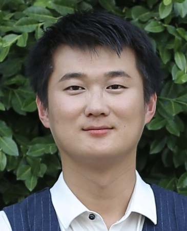 Kaisheng Ma (马恺声)合作论文数Institute for Interdisciplinary Information Sciences, Tsinghua University19Zhibo Wang合作论文数17
 Wenjun Tang合作论文数17
 Guodong Yin合作论文数BNRist, Tsinghua University, Beijing, China17
 Jingyu Wang (王敬宇)合作论文数School of Computer Science, Beijing University of Posts and Telecommunications;Network Intelligence Research Center, State Key Laboratory of Networking and Switching Technology, Beijing University of Posts and Telecommunications17
 Yiqun Wang (王逸群)合作论文数University of Chinese Academy of Sciences;Institute of Automation, Chinese Academy of Sciences17
 Hui Wang (王慧)合作论文数School of Environment, Tsinghua University17
 Jinyang Li (李金扬)合作论文数Department of Computer Science, New York University;Courant Institute of Mathematical Sciences, New York University17
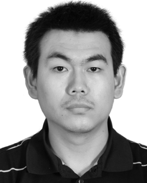 Daming Zhang合作论文数16Yinan Sun合作论文数16
 Yuxuan Huang合作论文数Department of Electronic Engineering, Tsinghua University15
 Zhuqing Yuan合作论文数Department of Electronic Engineering, Tsinghua University15
 Hehe Li合作论文数SZ DJI Technology Co., Ltd.15
 Rong Luo合作论文数15Mufeng Zhou合作论文数14
 Wenbin Jia合作论文数14Luchang Lei合作论文数13
 Yaolei Li合作论文数13Wenxun Wang合作论文数12
 Chunmeng Dou合作论文数Institute of Microelectronics of Chinese Academy of Sciences, Beijing, China12
 Tongda Wu合作论文数12
 Kai Ni合作论文数Department of Electrical Engineering, College of Engineering, University of Notre Dame;Department of Electrical and Microelectronic Engineering, Rochester Institute of Technology12Zongle Huang合作论文数11Zhonghao Chen合作论文数11
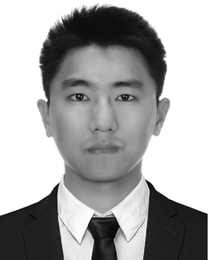 Qinghang Zhao合作论文数11
 Keni Qiu (邱柯妮)合作论文数Information Engineering College, Capital Normal University11
 Yanzhi Wang合作论文数Department of Electrical & Computer Engineering, College of Engineering, Northeastern University;Physical AI Research Center, Northeastern University;EmbodyX11Xinyuan Lin合作论文数10