High-efficiency power amplifiers (PAs) will be critical building-blocks for future sub-THz communications systems. InP heterojunction bipolar transistors (HBTs) with THz-class transistor bandwidth demonstrate PAs with high RF power density and high efficiency at frequencies between 100-300GHz. We review the performance of a state-of-the-art InP HBT IC technology and reported IC results that are applicable to future sub-THz communications systems.
We report on GaN-based field effect transistors with laterally-gated multiple 2DEG channels, called BRIDGE FETs (buried dual gate FETs). Unique operation principle of the transistors demonstrated unprecedented device characteristics suitable for efficient and linear millimeter-wave power amplifier applications. Multiple 2DEG channels formed in AlGaN/GaN and AlN/GaN material systems are compatible with the BRIDE FET structure, adding design flexibility for an increased drain current density with higher frequency performance. The BRIDGE FET fabricated on a 4-channel epi structure with a net 2DEG density of 1.2×10 13 cm -2 exhibited 1.7× higher saturation current density than those on a single-channel with the same 2DEG density. This is attributed to a higher saturation velocity of 2DEG with a lower density per channel. Finally, hexagonal micro-scale device cells consisting of segmented BRIDGE FETs construct a power amplifier (PA) unit cell, where distributing heat sources uniformly over an entire PA cell area maximizes its area power density while minimizing a rise of the peak junction temperature.
Highly-scaled Indium Phosphide (InP) transistor technologies have bandwidths extending into the terahertz (THz) frequency regime (0.3-3 THz). The high transistor bandwidth can be exploited to both extend circuit operation to THz frequencies and improve system performance at millimeter wave and sub-millimeter wave frequencies. InP heterojunction bipolar transistor (HBT) technologies offer wide bandwidths, high RF power handling and the capability to realize high levels of integration. We review integrated circuit (IC) results from Teledyne's InP HBT technologies that span frequencies from 60 GHz to >600 GHz focusing on performance benefits and applications.
Through aggressive lithographical and epitaxial scaling, the bandwidths of InP-based heterojunction bipolar transistors have been extended to THz frequencies. At 130nm emitter dimensions, transistors with maximum frequencies of oscillation (f max ) of >1THz have been demonstrated with accompanying circuit demonstrations at 670GHz. At 250nm emitter dimensions, high efficiency and high power density mm-wave power amplifiers covering E-band (71GHz) to G-band (235GHz) have been fabricated. The utility of these high performance transistors can be further enhanced through heterogeneous integration with Si CMOS. We have demonstrated wafer-scale 3D integration of InP and Si using a low temperature oxide-to-oxide bonding process with embedded Cu interconnects.
With transistors approaching scaling limits, demonstrating a record device demands ∼20–40 process steps, many at extreme resolution. Facing this, how might a Ph.D. student steer the future of VLSI or of wireless systems? Beyond exploring yet more new channel materials, whether 2D or 3D, we explore below other options.
High-mobility III-V transistors are poised to take the lead on future high performance logic operation. If this happens, indium-rich InxGa1-xAs is the most promising n-channel material. Indeed, remarkable progress has been made, including III-V gate-stacks with ALD-grown gate dielectrics. This paper reviews the evolution of high-performance III-V devices for future logic applications and discuss a possible path forward to further improve their logic figure-of-merits.
While the growth of III-As and III-P semiconductors is well-established, and their transport properties well-understood, the performance of high-frequency and VLSI electron devices can still be substantially improved. Here we review design principles, experimental efforts, and intermediate results, in the development of nm and THz electron devices, including nm InAs/InGaAs planar MOSFETs and finFETs for VLSI, InGaAs/InP DHBTs for 0.1-1 THz wireless communications and imaging, and ~5nm InAs/InGaAs Schottky diodes for mid-IR mixing.
A report is presented on 100 nm and 200 nm InAs PHEMTs on an InP substrate with a record f(T) performance. This result was obtained by reducing a parasitic delay associated with the extrinsic gate capacitances of the device, as well as by using an InAs sub-channel to improve carrier transport properties. In particular, a 100 nm InAs PHEMT exhibits excellent performance, such as g(m,max) = 2 S/mm, f(T) = 421 GHz and f(max) = 620 GHz at V-DS = 0.7 V. The device also shows a well-balanced f(T) and f(max) in excess of 400 GHz, even at V-DS = 0.5 V. In addition, the device gains about 70 % improvement in f(T) as L-g shrinks down from 200 to 100 nm. The results obtained in this work should make this technology of great interest to a multiplicity of applications and guide a realistic path in trying to achieve a 1 THz f(T) from III-V HEMTs in the future.
We have successfully demonstrated a three-step recess process to fabricate high performance E-mode planar InGaAs MOSFETs. Our devices feature a composite gate insulator with InP/Al2O3/HfO2. An Lg=35 nm InGaAs MOSFET with EOT = ~ 0.8 nm exhibits VT = 0.17 V, RON = 285 Ohm-μm, DIBL = 135 mV/V and S = 115 mV/dec, as well as a negligible dispersion and hysteresis behavior. Most importantly, our device displays the highest value of gm_max > 2 mS/μm at VDS = 0.5 V in any III-V MOSFETs.
In this Letter, we report on sub-100 nm recessed In0.7Ga0.3As metal-oxide-semiconductor field-effect transistors (MOSFETs) with outstanding logic and high-frequency performance. The device features ex-situ atomic-layer-deposition (ALD) 2-nm Al2O3 layer on a molecular-beam-epitaxy (MBE) 1-nm InP layer and is fabricated through a triple-recess process. An Lg = 60 nm MOSFET exhibits on-resistance (RON) = 220 Ω-μm, subthreshold-swing (S) = 110 mV/decade, and drain-induced-barrier-lowering (DIBL) = 200 mV/V at VDS = 0.5 V, together with enhancement-mode operation. More importantly, this device displays record maximum transconductance (gm_max) = 2000 μs/μm and current-gain cutoff frequency (fT) = 370 GHz at VDS = 0.5 V, in any III-V MOSFET technology.
A report is prsented on recessed QW In0.7Ga0.3As MOS-HEMTs with excellent subthreshold characteristics that combine an ALD-grown 3 nmAl(2)O(3) and an MBE-grown 10 nm In0.52Al0.48As barrier as a composite gate insulator. In particular, an L-g = 150 nm In0.7Ga0.3As MOS-HEMT exhibits V-T = -0.3 V, g(m_max) = 0.68 S/mm, DIBL = 35 mV/V and S = 70 mV/decade at V-DS = 0.5 V. To the knowledge of the authors, the subthreshold characteristics demonstrated are the best ever reported for any planar III-V MOSFET with similar values of L-g.
Scaling laws and limits of THz indium Phosphide heterojunction bipolar transistors (HBTs) are presented. The primary limits to scaling through the 32 nm / 3 THz node are the resistivity, penetration depth, and current-carrying capability of the emitter and base contacts. A processes flow with refractory dry-etch emitter and base contacts is presented. Beyond the 32 nm node, degenerate injection in the emitter-base junction limits transconductance and impedes scaling. At the 32 nm node, bandwidths will be sufficient for 1.4 THz transmitters and receivers.
We have successfully demonstrated a three-step recess process to fabricate high performance E-mode planar InGaAs MOSFETs. Our devices feature a composite gate insulator with InP/Al 2 O 3 /HfO 2 . An L g =35 nm InGaAs MOSFET with EOT = ∼ 0.8 nm exhibits V T = 0.17 V, R ON = 285 Ohm-μm, DIBL = 135 mV/V and S = 115 mV/dec, as well as a negligible dispersion and hysteresis behavior. Most importantly, our device displays the highest value of g m_max > 2 mS/μm at V DS = 0.5 V in any III-V MOSFETs.
Short-period (InAs)6/(AlSb)6 superlattices (SL) with AlAs-like and InSb-like interfaces (IF) grown on a relaxed AlSb buffer layer are studied by X-ray reflectivity and diffractometry measurements. Reflectivity measurements reveal average IF roughnesses between 0.6 and 1.0 nm. Measurements of the diffuse scattering show that the roughness is highly correlated from layer to layer. Triple crystal area scans illustrate that the inhomogeneous deformation of the buffer layer leads to a certain symmetric peak broadening. In the case of AlAs-like IFs an additional broadening of the SL peaks reveals lattice parameter gradients over the superlattice. This asymmetric peak broadening may be attributed to a further relaxation of the superlattice, which is inhomogeneous with depth. The diffusion of As into the AlSb layers leads to a peak shift and modifies the intensity ratios of the different satellite reflections. The best structural quality is achieved for superlattices with InSb-like IFs.
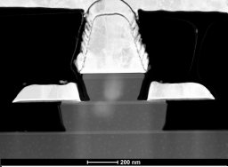
Fig. 1. Cross-section of self-aligned base-emitter junction from Teledyne 500nm HBT process [6] InP-based transistor technologies, both high electron mobility transistors (HEMTs) and double heterojunction bipolar transistors (DHBTs), have demonstrated the highest reported transistor RF figures-of-merit. Both device technologies have been reported with current gain cutoff frequencies (ft) in excess of 600GHz [1,2], and power gain cutoff frequencies (fmax) in excess of 1THz [3,4]. These performance records are achieved because of the inherent advantages of the InP/InGaAs material system (high electron mobilities/velocities, low attainable Ohmic contact resistivities and large heterojunction offsets), and through aggressive transistor scaling. With their wideband gap InP collector InP DHBTs offer a higher breakdown voltage than InGaAs-channel HEMTs at the same ft. Their high-speed and high-voltage handling make HBTs suitable for a wide breadth of applications including: sub-mm-wave and THz frequency integrated circuits, >100Gbit/sec optical and wireless communication circuits, microwave operational amplifiers, and high resolution microwave frequency analog-to-digital and digital-to-analog converters. In this paper, we review HBT and IC results from Teledyne Scientific Company’s InP HBT technology. A scalable device architecture has been developed and successive generations of the technology have been demonstrated (500nm to 130nm). Increased functionality of the technology is being pursued with the development of a BiFET (HBT+HEMT) InP technology and through heterogeneous integration with Silicon CMOS.
We have demonstrated 40-nm In0.7Ga0.3As Metamorphic HEMTs (MHEMTs) with a record value in fT. The devices feature a Pt gate sinking process to effectively thin down the In0.52Al0.48As barrier layer, together with dual Si d-doping in the barrier to lower the potential barrier in the S/D access region. The fabricated device with Lg = 40-nm exhibits VT = 0.05 V, gm,max = 2.7 mS/μm, fT = 688 GHz and fmax = 800 GHz. In addition, we have developed an analytical model of fT in a III-V HEMT based on a small-signal equivalent circuit, which provides an excellent agreement with measured fT. This in turns guides a realistic way to further improve fT beyond THz. . Introduction The last several years have witnessed an explosion of interest in devices suitable for ultra high frequency applications, such as in the Tera-Hz regime. In particular, InGaAs-based high-electron mobility transistors (HEMTs) and heterojunction bipolar transistors (HBTs) have shown great success in microwave and millimeter-wave applications, and are now considered the best candidates for future THz electronics [1-4]. These remarkable results have been achieved through the combination of downscaling of minimum feature size, parasitics reduction, and the use of a channel material with very high electron velocity. In this paper, we report on E-mode Lg = 40 nm In0.7Ga0.3As metamorphic-HEMTs (MHEMTs) on GaAs substrate with a record fT = 688 GHz, which to the knowledge of the authors, is the highest ever reported in any FET on any material system. In addition, we have constructed a simple and analytical model for fT based on a small-signal equivalent circuit and shown that very high intrinsic transconductance (gmi) in excess of 4 mS/μm in our Lg = 40 nm device is effective in mitigating a parasitic charging delay associated with the extrinsic gate capacitances. This greatly contributes to the record value of fT in our Lg = 40 nm MHEMTs. Process Technology Fig. 1 shows cross section and TEM images of the fabricated InGaAs MHEMTs on GaAs substrate. From top to bottom, the epitaxial layer structure consists of a heavily doped multi-layer cap (In0.7Ga0.3As/In0.53Ga0.47As/In0.52Al0.48As), 6nm InP etch-stopper, 2-nm In0.52Al0.48As barrier, upper Si δdoping, 6-nm In0.52Al0.48As barrier, lower Si δ-doping, 2-nm In0.52Al0.48As spacer, 1-nm In0.7Al0.3As spacer, 10-nm In0.7Ga0.3As channel, 300-nm In0.52Al0.48As buffer and 0.3 μm graded metamorphic buffer on GaAs substrate. A dual Si δdoping and an In0.7Al0.3As spacer were utilized to lower the potential barrier in the access regions and reduce the parasitic resistance. The device fabrication is almost identical to [1]. After a two-step recess process that exposes an InAlAs barrier, a Pt/Ti/Pt/Au gate was created. Subsequently, the devices were annealed at 250 °C for 2 minutes to drive the Pt into the InAlAs barrier. In this way, a gate-to-channel distance (tins) of about 4-nm was achieved. The gate stem height was increased to 250 nm to mitigate the fringing capacitance of the T-gate. From the TEM images, the physical Lg, and side-recessspacing (Lside) were 40 nm and 100 nm, respectively. Fig. 1 Schematic of InGaAs MHEMTs and TEM images of the fabricated Lg = 40 nm device. It features 0.3 μm graded metamorphic buffer on GaAs substrate. The device brings unique aspects to mitigate parasitics and short-channel effects. The physical Lg and side-recess spacing (Lside) were 40 nm and 100 nm, respectively. 13.6.1 IEDM11-319 978-1-4577-0505-2/11/$26.00 ©2011 IEEE DC & Microwave Characteristics Figs. 2 and 3 show output and transconductance (gm) characteristics of an Lg = 40 nm InGaAs MHEMT. The device exhibits excellent pinch-off and drain current saturation behavior up to VDS = 0.8 V. The device is enhancement-mode with VT = 0.05 V. A very small value of RON = 280 Ω-μm is obtained, mainly due to the dual Si δdoping and the InAs-rich In0.7Al0.3As spacer. As a consequence, the device has outstanding gm_max = 2.75 mS/μm at VDS = 0.8 V, and in excess of 2 mS/μm even at VDS = 0.3 V, both of which make our device technology attractive for high-performance and very low-power applications. 0.0 0.2 0.4 0.6 0.8 1.0 0.0 0.4 0.8 1.2
 Miguel E. Urteaga合作论文数Advanced Device Development Group, Teledyne Scientific Company37
 Joshua Bergman合作论文数24
 Mark Rodwell合作论文数Department of Electrical and Computer Engineering, University of California, Santa Barbara24
 Herbert Kroemer合作论文数University of California, Santa Barbara21Richard Pierson合作论文数19Petra Rowell合作论文数18
 Zach Griffith合作论文数Department of Electrical and Computer Engineering, University of California at Santa Barbara16
 Arthur Gossard合作论文数College of Engineering, University of California, Santa Barbara14
 Clark T. C. Nguyen合作论文数Berkeley Sensor & Actuator Center, University of California Berkeley;Department of Electrical Engineering and Computer Sciences, University of California Berkeley13
 Gabor Nagy合作论文数12
 J. B. Hacker合作论文数Division of Tropical Crops and Pastures, CSIRO12
 C. Kadow合作论文数12
 Alan Seabaugh合作论文数Department of Electrical Engineering, College of Engineering, University of Notre Dame11
 Heng-Kuang Lin合作论文数9Jh English合作论文数8
 Daehyun Kim合作论文数Dept Atmospher Sci, Univ Washington8
 M. Dahlstrom合作论文数Department of Electrical and Computer Engineering;University of California , Santa Barbara;Department of Electrical and Computer Engineering, University of California , Santa Barbara8Dmitri Lubyshev合作论文数7Liu, W.K.合作论文数7Wonill Ha合作论文数7
 Mayank Bulsara合作论文数Taiyo Nippon Sanso Innovation7
 Jesús A. Del Alamo合作论文数Department of Electrical Engineering and Computer Science, Massachusetts Institute of Technology7Joel M. Fastenau合作论文数7
 Eugene A. Fitzgerald合作论文数Materials Research Laboratory, Massachusetts Institute of Technology;4Power LLC;New Silicon Corporation Pte. Ltd;Paradigm Research LLC7
 Navin Parthasarathy合作论文数7Gregory T Sullivan合作论文数6
 Nicolas Daval合作论文数6
 Achim Wixforth合作论文数Institut für Physik, Universität Augsburg6Ch Gauer合作论文数6
 Jörg Peter Kotthaus合作论文数Fakultät für Physik, Ludwig-Maximilians-Universität München6
 Keisuke Shinohara合作论文数Institute of Fluid Science, Tohoku University6Charlotte Drazek合作论文数6t e kazior合作论文数5J. R. LaRoche合作论文数5w e hoke合作论文数5Tae-Woo Kim合作论文数5a papavasiliou合作论文数5
 Dimitri Antoniadis合作论文数Department of Electrical Engineering and Computer Science, Massachusetts Institute of Technology;Microsystems Technology Laboratories, Massachusetts Institute of Technology5Pinsukanjana, Paul合作论文数5J.M. Kuo合作论文数5F. Morris合作论文数4
 L. Benaissa合作论文数4
 Colombo Bolognesi合作论文数Millimeter Wave Elect Grp, ETH4
 Klaus Ensslin合作论文数Department of Physics, Eidgenössische Technische Hochschule Zürich4M. Thomas合作论文数4
 G. J. Sullivan合作论文数4
 Mark Field合作论文数Department of Cardiothoracic Surgery, Nottingham City Hospital4




