Low-pass filters with bandwidths larger than several GHz are required in many applications, such as anti-aliasing filters in high-speed ADCs and pulse-shaping filters in high-speed DACs. In highly integrated applications, low area occupation and power consumption are key specifications, so inductor-less implementations are to be preferred. Furthermore, full CMOS implementations provide an advantage in terms of technology availability and cost. In this paper, we present an inductor-less CMOS biquad stage based on the super source follower topology that provides an 8 GHz cutoff frequency and a low power consumption of 0.42 mW per pole, showing remarkable performance also in terms of bandwidth and dynamic range. The availability of two separate current sources allows independent tuning of natural frequency and quality factor. The stage can be implemented in two complementary ways, exploiting NMOS and PMOS input devices, respectively, thus simplifying cascadability. The two complementary biquads have been implemented in the STMicroelectronics FDSOI 28 nm CMOS process and extensively simulated and provide stable performance under PVT variations and mismatches. The area occupation is about 387.5 μm2 per biquad, one of the lowest in the literature. The figures-of-merit are remarkable, as the filters achieve excellent power efficiency, very low area occupation, and good dynamic range.
Biomedical sensors operate under low supply voltage, in low frequency domains, and require low power consumption. This paper proposes a new power-efficient, low-pass and band-pass fully differential biquad suitable for bio-signal acquisition, based on Folded Gain Boosting Source-Follower (FGB-SF). This solution does not require a Common-Mode Feedback (CMFB) and it offers a wide tuning range. Implemented using 0.18 mu m TSMC technology, it achieves the lowest power consumption reported in the literature (0.46 nW), a high Dynamic Range (DR) of 43.8 dB, and an IIP3 of 6.55 dBm with 250 Hz bandwidth. Post-layout simulations demonstrate stability under Montecarlo and PVT variations. The occupied area is only 69.5 mu m x 51.3 mu m and exibits the lowest FOM compared with the state of the art.
In this paper, we present the design and the experimental validation of a biquad filter for biomedical applications that takes advantage of segmented duty-cycled resistors to allow for digital tuning over a wide range of the cutoff frequency (f0), quality factor (Q), and gain (K). Additionally, we report on the experimental findings for an 8th-order band pass filter that was created to extract the epilepsy biomarker, related to the fast ripple band (250 Hz–500 Hz). The results of measurements on a prototype chip, implemented in a commercial 130 nm CMOS technology with a supply voltage of 0.5 V and a power consumption of 120 nW, confirm that the f0 of the proposed biquad filter can be digitally tuned from 15 Hz up to 517 Hz, whereas the Q can be tuned from 0.7 up to 13. A comparison against the state of the art has shown that the proposed biquad filter exhibits the lowest area, with the highest Q, and can be tuned at the lowest f0. It also exhibits the unique feature to allow for independent tunability of f0, Q, and K by varying the duty-cycle of digital control signals. The 8th-order filter, implemented with 4 cascaded instances of the proposed biquad filter, guarantees an attenuation higher than 30 dB at f0/2 and 2f0 with a power consumption of 480 nW, and an area footprint of 0.152 mm2, thus satisfying the requirements to extract the epilepsy biomarker in closed-loop deep brain stimulation systems.
This paper presents a low-power and area-efficient chopper-stabilized low noise amplifier (CS-LNA) for in-pixel neural recording systems. The proposed CS-LNA can be used in a multi-channel architecture, in which the chopper mixers of the LNA are exploited to provide the time division multiplexing (TDM) of several channels, while reducing the flicker noise and rejecting the Electrode DC Offset (EDO). A detailed noise analysis including the effect of the chopper stabilization on flicker noise, and a design flow to optimize the trade-off between input-referred noise and silicon area are presented, and utilized to design the LNA. The adopted approach to reject the EDO allows to tolerate an input offset of ±50 mV, without appreciably affecting the CS-LNA performance, and does not require an additional DC Servo Loop (DSL). The proposed CS-LNA has been fabricated in a 0.13 μm CMOS process with an area of 0.0268 mm2, consuming about 2 μA from a 0.8 V supply voltage. It achieves an integral noise of 4.19 μVrms (2.58 μVrms) from 1 to 7.5 kHz (from 300 to 7.5 kHz) and results in a noise efficiency factor (NEF) of 2.63 (1.62). Besides achieving a maximum gain of 38.67 dB with a tuning range of about 12 dB, the neural amplifier exhibits a CMRR of 67 dB. A comparison with the recent literature dealing with in-pixel amplifiers shows state-of-the-art performance.
An approach to design analog building blocks based on digital standard cells is presented in this work. By ensuring that every CMOS inverter from a standard-cell library operates with a well-defined quiescent current and output voltage, the suggested method makes it possible to construct analog circuits that are resistant against PVT variations. The method uses the local supply voltages connected to the source terminals of the p-channel and n-channel MOS transistors of the standard-cell inverters as control inputs. It is based on adaptive supply voltage generator (ASVG) reusable blocks, which are comparable to those used in digital applications to handle process variations. All of the standard-cell inverters used for analog functions receive the local supply voltages produced by the ASVGs, which enable setting each cell’s quiescent current to a multiple of a reference current and each cell’s static output voltage to an appropriate reference voltage. Both the complete custom design of the ASVG blocks and a theoretical study of the feedback loop of the ASVG are presented. An application example through the design of a fully synthesizable two-stage operational transconductance amplifier (OTA) is also provided. The TSMC 180 nm CMOS technology has been used to implement both the OTA and the ASV generators. Simulation results have demonstrated that the proposed approach allows to accurately set the quiescent current of standard-cell inverters, dramatically reducing the effect of PVT variations on the pmain performance parameters of the standard-cell-based two-stage OTA.
The technology transfer of terahertz wireless communication from research laboratories to commercial applications is a global strategic achievement currently pursued to match the ever-increasing demand for high-speed communication. The use of commercial integrated electronics for the detection of THz waves is an intriguing challenge which has enticed great interest in the scientific research community. Rapid progress in this field has led to the exploitation of THz direct detection using standard CMOS technology based on the so-called self-mixing effect. Our research, stemming out of a collaboration between Sapienza University of Rome and STMicroelectronics company, is focused on the complete design process of a THz rectifier, realized using 50 nm ST B55 CMOS technology. In this paper, we report the optimization process of a case-study receiver, aimed to demonstrate the feasibility of direct demodulation of the transmitted OOK signal. A relatively limited bandwidth extension is considered since the device will be included in a system adopting a radiation source with a limited band. The design refers to a specific technology, the 60 nm MOS in B55X ST; nevertheless, the proposed optimization procedure can be applied in principle to any MOS device. Several aspects of the rectification process and of the receiver design are investigated by combining different numerical simulation methodologies. The direct representation of the rectification effect through the equivalent circuit of the detector is provided, which allows for the investigation of the detector–amplifier coupling, and the computation of output noise equivalent power. Numerical results are presented and used as the basis for the optimization of the receiver parameters.
In this work a novel technique to design ultra-low voltage (ULV), ultra-low power (ULP), inverter-based OTAs is presented. The proposal consists in utilizing a replica bias control loop applied to a body-driven inverter stage, with the aim of accurately setting both the DC current and the static output voltage, thus also centering the voltage transfer characteristic of the inverter cell. The proposed custom body-driven inverter attains rail-to-rail input common mode range, even at supply voltages as low as 0.3 V, and exhibits very stable performance under process, supply voltage and temperature (PVT) variations. The body-driven inverter cell is then exploited to implement a ULV, ULP OTA with small silicon area footprint, whose supply voltage can be scaled down to 0.3V. An extensive simulation campaign in a 180 nm CMOS technology has shown state-of-the-art performance in terms of small signal figure of merits, attaining very good robustness with respect to PVT variations.
In this work, a novel technique to feed body-driven ultra-low voltage (ULV) comparators is investigated to enhance performance in terms of noise and offset. The technique, which consists in clocking the supply voltage of the latch devices, causes the output common mode voltage to experience a positive step at the beginning of the evaluation phase. As a result, the preamplification gain is enhanced because the output nodes are discharged for a longer time before the latch turns on. The proposed approach is validated by applying it to an ULV comparator topology proposed in a previous work. Post-layout simulation results on a 130nm node demonstrate that input-referred noise and offset improve approximately 20% and 15%, respectively, while the energy-delay product of the comparator EDP remains essentially unchanged.
This paper introduces an innovative approach to designing a mismatched current mirror with a fully unbalanced output, significantly reducing the minimum supply voltage requirements for Regulated Cascode Current Mirror (RCCM) Physical Unclonable Functions (PUFs). Leveraging body-driven feedback mechanisms, the proposed circuit reliably operates with supply voltages as low as 0.3V, maintaining stable power consumption through a reference bias current. The resulting PUF achieves remarkable energy efficiency, consuming only 0.3 fJ per bit, without compromising statistical performance. It exhibits a response bias of 49.42%, a reliability of 99.483%, and a uniqueness of 50.176%. Validation of this novel approach is conducted through simulations and measurements on a 130nm CMOS test-chip, considering a nominal supply voltage of 0.3V, +/- 10% supply voltage variations, and a temperature range from 0degree celsius to 75degree celsius. Rigorous experimental verification on 20 chip samples, along with detailed explanations of design methodologies, underscores the robustness and practicality of the proposed Body-PUF design. Comparative analyses against state-of-the-art literature reveal that the Body-PUF outperforms previous PUF designs in Figures of Merit (FOM), making it promising for real-world authentication scenarios. Its outstanding trade-off between performance and practicality positions it as a compelling solution for secure applications, including Internet of Things (IoT) devices and other security-critical systems.
This work proposes a novel switching algorithm for capacitive digital-to-analog converters (CDAC) in successive approximation register (SAR) analog-to-digital converters (ADC). The proposed CDAC requires the same number of capacitors and switches as the monotonic switching CDAC while achieving a much smaller output common mode swing. This is obtained by properly alternating upwards and downwards transitions in the CDAC and by temporarily shifting the output common mode voltage. In addition, the common mode voltage to which the CDAC outputs converge can be decoupled from the input common mode of the ADC. As a result, the performance of the converter improves significantly because the behavior of the CDAC can be tailored according to the optimum input common mode of the comparator. The only cost is a slight increase of the average power consumption. The proposed technique has been validated by applying it to a 10 bit, 150 MS/s SAR ADC implemented in a 55 nm technology by STMicroelectronics. Despite the absence of calibration and redundant encoding, the ADC exhibits a signal-to-noise-and-distortion ratio (SNDR) of 56.3 dB while consuming 5.7 mW from a 1 V supply.
In this work, we introduce the design of a 16-channel in-pixel neural analog front end that employs a current-based summing approach to establish a common-mode feedback loop. The primary aim of this novel structure is to enhance both the system common-mode rejection ratio (SCMRR) and the common-mode interference (CMI) range. Compared to more conventional designs, the proposed front end utilizes DC-coupled inverter-based main amplifiers, which significantly reduce the occupied on-chip area. Additionally, the current-based implementation of the CMFB loop obviates the need for voltage buffers, replacing them with simple common-gate transistors, which, in turn, decreases both area occupancy and power consumption. The proposed architecture is further examined from an analytical standpoint, providing a comprehensive evaluation through design equations of its performance in terms of gain, common-mode rejection, and noise power. A 50 μm × 65 μm compact layout of the pixel amplifiers that make up the recording channels of the front end was designed using a 180 nm CMOS process. Simulations conducted in Cadence Virtuoso reveal an SCMRR of 80.5 dB and a PSRR of 72.58 dB, with a differential gain of 44 dB and a bandwidth that fully encompasses the frequency range of the bio-signals that can be theoretically captured by the neural probe. The noise integrated in the range between 1 Hz and 7.5 kHz results in an input-referred noise (IRN) of 4.04 μVrms. Power consumption is also tested, with a measured value of 3.77 μW per channel, corresponding to an overall consumption of about 60 μW. To test its robustness with respect to PVT and mismatch variations, the front end is evaluated through extensive parametric simulations and Monte Carlo simulations, revealing favorable results.
Forward body biasing (FBB) has often been exploited in the literature for improving the performance of both analog and digital building blocks. Recent works have explored the application of FBB variants to mixed-signal electronics and in particular to dynamic comparators, where these techniques can help to relax the trade-off between speed and power consumption at medium and low supply voltages. However, the literature lacks a structured analysis of the solutions that have been developed and of the trade-offs that affect them. This work attempts to fill the gap by providing a survey of the application of FBB techniques to dynamic comparators. The analysis focuses on the two most popular dynamic comparator topologies, the Strong Arm latch and Elzakker’s comparator. Several FBB variants are examined from a theoretical point of view. Moreover, the benefits and the limitations of the different approaches are assessed in terms of the main figures of merit through a systematic campaign of simulations in a 55 nm CMOS technology.
Inductor-less CMOS filters with bandwidth exceeding several GHz are required in high-speed data converter applications. This paper introduces two complementary biquad filters, one N-based and the other P-based, utilizing the well-established flipped voltage follower (FVF) stage. These filters exhibit more than 7 GHz cut-off frequency and a low power consumption of 0.54 mW/pole for the N-type biquad, and 0.3 mW/pole for the Ptype one, demonstrating impressive figures-of-merit (FOMs) even considering bandwidth and dynamic range. The implementation of these biquads in the STMicroelectronics FD-SOI 28-nm CMOS process, along with extensive simulations, ensures stable performance under process, supply voltage and temperature (PVT) variations and mismatches, as confirmed by post-layout simulations. Notably, the area occupied by each biquad is merely 246 mu m2 2 for N-type biquad and 193 mu m2 2 for P-type, marking one of the smallest footprints in the existing literature. The achieved figures-of-merit are noteworthy, showcasing excellent power efficiency, minimal area occupation, and commendable dynamic range.
In this paper we introduce an improved standard-cell-based voltage amplifier cell with low output resistance. The proposed amplifier cell exhibits a voltage gain whose value can be accurately set by the number of paralleled inverters, and its output static voltage is well controlled through a replica bias approach. A three-stage fully synthesizable OTA architecture exploiting the improved voltage amplifier is also proposed. The OTA has been designed referring to the standard-cell library of a 180nm CMOS technology with a supply voltage of 0.3V and a nominal power consumption of only 6.63 nW, and exhibits a dc-gain of 73.5 dB with a gain-bandwidth-product of 9.63 kHz. A comparison against the state of the art of ultra-low-voltage OTAs has shown that the proposed amplifier exhibits the best value of the small signal figures of merit.
In this paper, we present a 0.3 V body-driven operational transconductance amplifier (OTA) that exploits a biasing approach based on the use of a replica loop with gain. An auxiliary amplifier is exploited both in the current mirror load of the first stage of the OTA and in the replica loop in order to achieve super-diode behavior, resulting in low mirror gain error, which enhances CMRR, and robust biasing. Common-mode feedforward, provided by the replica loop, further enhances CMRR. Simulations in a 180 nm CMOS technology show 65 dB gain with 2 kHz unity-gain frequency on a 200 pF load when consuming 9 nW. Very high linearity with a 0.24% THD at 90% full-scale and robustness to PVT variations are also achieved.
In the last years several ultra-low voltage (ULV) operational transconductance amplifiers (OTAs) with supply voltages below 0.5V have been proposed in the literature. To achieve high gain, multi-stage amplifiers are frequently exploited, in spite of the complexity of design and compensation approaches, whereas cascode and regulated-cascode OTA topologies have rarely been exploited to implement ULV amplifiers. On the other hand, most ULV amplifiers are designed for IoT and biomedical applications in which reducing power consumption is the most important specification, and MOS devices are operated in the subthreshold region. This paper focuses on exploiting the subthreshold operating region to design ULV single-stage OTAs that utilize an output cascoded branch to increase the equivalent output resistance and, consequently, the overall voltage gain. A detailed analytical study of the conditions for triode and saturation regions for MOS devices operating in deep subthreshold region is presented to demonstrate that, for an appropriate choice of the inversion coefficient (IC), a cascode configuration exhibits higher gain than a single transistor, for the same voltage overhead, even in ULV conditions. More specifically, the results presented in this work demonstrate that 4 MOS devices (2 NMOS and 2 PMOS) can be reliably stacked to build a complementary cascode amplifier, even with a supply voltage as low as 0.4V. We also present a novel topology of regulated-cascode amplifier suitable to be operated with a supply voltage of 0.4V and a voltage gain approaching 100dB. Simulation results referring to a 180nm CMOS technology and including PVT and mismatch variations confirm state-of-the-art performances, as well as the good robustness of the proposed regulated-cascode ULV OTA.
In this paper a novel ultra-low voltage (ULV) standard-cell-based comparator which provides rail-to-rail input common-mode range (ICMR) is presented. The topology, unlike the others in the literature, uses only 2-inputs NAND gates and is able to operate with supply voltages as low as 0.15V. A detailed theoretical analysis based on transistor level modeling is provided to explain the operating principle and highlight the performance advantages of the proposed comparator. The circuit has been tested through several simulations, including corner analysis and Monte Carlo runs, by using three different technologies: 180 nm, 130 nm and 28 nm for both a supply voltage of 0.3 V and 0.15 V. The results found not only confirm the robustness of the proposed comparator, but also demonstrate very advantageous performances. Indeed, for the same technology node it exhibits the highest speed and the lowest EDP (about ten times lower than the one of the others standard-cell-based comparators in the literature). It exhibits also the lowest power consumption and silicon area.
In this work a novel ultra-low voltage, ultra-low power fully synthesizable comparator is presented. The proposed architecture exploits only 2-input NAND gates, that allow minimization of the area footprint and scalability up to extremely low supply voltages. An extensive simulation campaign in a 130 nm CMOS technology has shown state-of-the-art performance in terms of power-delay-product for supply voltages down to 0.3V. Simulations also show good robustness under mismatch and PVT variations, proving the feasibility of the approach.
 Alessandro Trifiletti合作论文数Dipartimento di Ingegneria Elettronica, Università di Roma "La Sapienza",144
 Giuseppe Scotti合作论文数Dipartimento di Ingegneria Elettronica, Universita di Roma "La Sapienza"83
 Pietro Monsurro合作论文数Dipartimento di Ingegneria Elettronica, Università di Roma "La Sapienza",64
 Pasquale Tommasino合作论文数53
 Riccardo Della Sala合作论文数Dipartimento Ingn Informaz Elettron & Telecomunica, Univ Roma La Sapienza32
 Cristian Bocciarelli合作论文数11
 Valerio Spinogatti合作论文数11
 Alessandro Fava合作论文数Dipartimento di Ingegneria dell’Informazione, Elettronica e Telecomunicazioni, Universitá degli Studi di Roma La Sapienza10
 Raimondo Luzzi合作论文数Infineon Technologies AG10
 Vincenzo Stornelli合作论文数Department of Industrial and Information Engineering and Economics, Università degli Studi dell'Aquila9
 Giuseppe Ferri合作论文数Dipartimento di Ingegneria industriale e dell'informazione e di economia, Università degli Studi dell'Aquila9
 Leonardo Pantoli合作论文数Department of Electrical and Information Engineering, University of L'Aquila8
 Marco Balsi合作论文数Department of Information Engineering, Electronics and Telecommunications, Sapienza University of Rome;Universitat Ramon Llull;Hungarian Academy of Sciences;Università Degli Studi Roma Tre8
 Gianluca Barile合作论文数Univ Aquila, Dept Ind & Informat Engn & Econ, I-67100 Laquila, Italy7
 Gaetano Palumbo合作论文数Dipartimento di Ingegneria Elettrica Elettronica e dei Sistemi, Universita di Catania7
 Pennisi, S.合作论文数5
 Pallotta, A.合作论文数5
 Salvatore Pennisi合作论文数Department of Electrical Electronic and Computer Engineering, University of Catania5Andrea Pallotta合作论文数5
 Massimo Pozzoni合作论文数5
 Danilo Ruscio合作论文数Radio Analog Micro Elect Srl4
 Fabrizio Palma合作论文数Dipartimento di Elettronica, Università “La Sapienza”,4Alessandro Ercolani合作论文数4
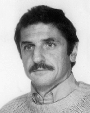 Piero Marietti合作论文数4
 Rosario Cimmino合作论文数3F. Romano合作论文数3
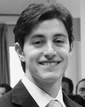 Gaetano Parisi合作论文数3
 Carmine Mustacchio合作论文数University of Calabria,Arcavacata di Rende (CS),87036 Italy3
 Davide Bellizia合作论文数Univ Roma La Sapienza, DIET, Rome, Italy3
 Pascal Chevalier合作论文数STMicroelectronics3
 Luigi Boccia合作论文数Dipartimento di Elettronica, Informatica e Sistemistica Via Bucci, Università della Calabria3
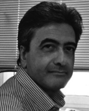 Giandomenico Amendola合作论文数Dipartimento di Elettronica, Informatica e Sistemistica Via Bucci, Università della Calabria3Alessandra Forte合作论文数3Andrea Simonetti合作论文数3Mario Olivieri合作论文数3
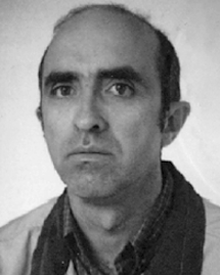 Jesus Guinea合作论文数2alessandro golfarelli合作论文数2
 Leonardo Masini合作论文数2
 Davide Colaiuda合作论文数2
 Paola Piedimonte合作论文数Department of Electronics Information and Bioengineering, Politecnico di Milano2antonio saitto合作论文数2
 Felice Rosato合作论文数Sapienza University of Rome, Italy2
 Mauro Olivieri合作论文数Department of Information Engineering, Electronics and Telecommunications, Sapienza University of Rome2
 Alberto di martino合作论文数Department of Orthopaedic and Trauma Surgery, Campus Bio-Medico University2
 Damiana Morigi合作论文数2
 Salvatore Levantino合作论文数Politecnico di Milano2
 Andrea Mazzanti合作论文数Dept Organ Chem A Mangini, Univ Bologna2Pisa, S.合作论文数1G. Barile合作论文数1




