Traditional scan test interfaces though general purpose (GP) IOs suffer from bandwidth limitations, contributing to increasing manufacturing test costs. Applying scan test through high speed IOs (i.e. SERDES) is a key interest area for the industry to overcome bandwidth limitations of traditional scan test, but is under the development in the industry today due to the need for compatible technologies across the entire ecosystem of EDA, ATE and IC designers. Guided by IEEE 1149.10, a group of pioneer engineers / users are deploying their robust and complete solutions. In this industry session, engineers from fabless, ATE and EDA companies are sharing their experiences in this area.
System-on-Chip (SoC) designs are increasingly difficult to test using traditional scan access methods without incurring inefficient test time, high planning effort, and physical design/timing closure challenges. The number of cores keeps growing while chip pin counts available for scan remain constant or decline, limiting the ability to drive cores concurrently. With increasingly commonplace tiling and abutment, the scan distribution hardware must be placed inside the cores, making balanced pipelining when broadcasting to identical cores difficult. optimizing test time requires analyzing all the cores and subsequently changing the test hardware in the cores. Internal shift speed constraints may limit the ability to shift data in and out of the chip at high rates. Differences in pattern counts or scan chain lengths between cores tested in parallel can result in padding and increased test time. SSN is a bus-based scan data distribution architecture designed to address all these challenges. It enables simultaneous testing of any number of cores even with few chip I/Os. It facilitates short test time by enabling high-speed data distribution, by efficiently handling imbalances between cores, and by supporting testing of any number of identical cores with a constant cost. It provides a plug-and-play interface in each core that is well suited for abutted tiles, and simplifies scan timing closure. This paper also compares the test cost and implementation productivity of SSN with those of Intel's Structural Test Fabric.
In this article we explore the world of diagnosis of digital semiconductors devices. After shortly outlining the technology behind diagnosis, the main part of this article describes key improvements to the basic diagnosis tools we knew from previous years. These improvements enable the failure analysis engineer as well as the yield analysis engineer to use diagnosis as a powerful software instrument supplementing his portfolio of tools. Throughout this article, we summarize several successful industrial applications of diagnosis. For example we recap applications where diagnoses helped reducing the search area for defect down to 3% of the original search area size; and in another case, diagnosis was used to improve at-speed tests, increasing the speed by 300MHz, plus several other cases.
in many cases, the main cause of yield loss is a specific layout pattern that is difficult to manufacture and is prone to causing an open or short defect. This situation is getting worse with advanced technology nodes due to small feature sizes and complex manufacturing processes. Volume scan diagnosis results are a rich data source for identifying such yield limiting layout patterns, but a big challenge is how to deal with an enormously large number of potential layout patterns to be considered for analysis and how to avoid over fitting. In this paper we present enhancements to the previously published root cause deconvolution technique for analyzing volume scan diagnosis data that enables it to overcome this and correctly, and automatically, determine the right layout patterns causing systematic yield loss. Also presented is an application to industrial data where a layout pattern identified by the new technique was validated by physical root cause analysis to be the dominant yield loss mechanism.
In this paper, we propose expanding the use of volume diagnostics to go beyond the identification of critical features to accurately estimate their FFRs. We present a case study where FFRs of a few critical features are identified using volume diagnostics. We also compare FFRs calculated from volume diagnostics to those extracted for the same feature on test structures, which validates our presented approach.
This paper focuses on the V4-2007 extension of the Standard Test Data Format (STDF). STDF has been used as the standard representation for logging test data from automatic test equipment (ATE). This format however lacked a key capability, i.e., storing scan test results. The V4-2007 extension of this standard, as described in this paper, provides details on its ability in efficiently storing scan test results. Thus this standard now provides a complete and unified repository to store the results of parametric tests, functional tests and scan tests, all in a consistent format to aid in fault diagnosis and yield learning. This has in turn simplified the test flow and tracking of all necessary data to ensure more time-efficient testing and failure diagnosis.
For many years semiconductor manufacturers have successfully ramped and improved yield using yield management systems (YMS) and physical failure analysis. However, with new and subtle defect types introduced at modern production nodes, and ever increasing demands for product quality and profitability, additional tools are required. A new yield analysis methodology using scan diagnosis analysis is used to improve process debug and yield monitoring. The motivation for applying diagnosis analysis is driven by scenarios in which true silicon performance may not exactly match simulation across PVT corners or where systematic defects are design-driven. In such cases, wafer-level bin maps provide limited resolution [1] for scan signatures, and trends in data may not be visible with raw pin/cycle/fail data from the automated test equipment (ATE).
An increase in subtle systematic defect mechanisms, smaller feature sizes, and more complex designs make it significantly more time consuming to identify the cause of yield loss using traditional methods. The challenge on the design side is to aim the efforts at the right yield issues. To hit a bull's eye rather than a black hole with our yield improvement efforts, we can leverage the wealth of information that hides in the manufacturing test results using a technique called diagnosis-driven yield analysis a technique described in this article.
This case study compares the FA success rate and turn-around time of traditional logic-only and true layout-aware scan diagnosis. It discusses the basic process flow, identifies key success factors, and evaluates physical FA and diagnostic test results obtained from six dies randomly selected from a 9.8 M-gate, seven-metal-layer ASIC manufactured in 90 nm technology. As shown, layout-aware diagnosis reduces the defect search area on the die, in some cases, by an order of magnitude, providing the means to diagnosis-driven yield improvements.
This paper introduces embedded deterministic test (EDT) technology, which reduces manufacturing test cost by providing one to two orders of magnitude reduction in scan test data volume and scan test time. The EDT architecture, the compression algorithm, design flow, experimental results, and silicon implementation are presented.
Musculoskeletal injuries represent an adverse event of strenuous physical activity. The aim of the present study was to identify pretraining factors that may predispose to such injuries. Risks of injury according to age, body composition, previous physical activity, physical fitness, use of smokeless tobacco (moist snuff) and smoking habits were determined in a population of 480 male conscripts in the army. Data were obtained by questionnaire, height and weight measurements, and from a 3000‐metre run test prior to a 10‐week period of basic military and physical training. Injuries were registered by doctors attached to the training camp. Every fourth conscript sustained one or more musculoskeletal injuries during the training period. Low back pain, overuse knee injuries, Achilles tendinitis, and sprains of joint capsules or ligaments were the most frequent diagnosis groups. Subjects aged 22 years and more, the least active persons before call‐up, those who thought they were less fit than the average, the slowest one‐third in the 3000‐metre run test, smokers of more than 10 cigarettes a day, and snuff‐takers suffered more injuries according to univariate analyses. Multiple logistic regression analysis showed that age, self‐assessed physical fitness and snuff‐taking were mutually independent risk factors of high statistical significance.
Musculoskeletal injuries occur frequently in connection with physical activity. More information was sought on pretraining factors that may predispose to such injuries. Data were obtained on the age, height, weight, aerobic fitness as measured by a 3000‐m run test, and health as assessed on the basis of a medical examination, of 912 male conscripts prior to an 8‐week period of basic military and physical training. Injuries were registered as they occurred by doctors attached to the training camp. Every fourth to fifth conscript suffered one or more musculo‐skeletal injuries during basic training. Achilles tendinitis, low back pain, periostitis or compartment syndromes, and overuse knee injuries were the most frequent diagnosis groups. In 74% of the injuries, a tentative cause was related to organized service activities. According to univariate analyses, risk factors were age over 23 years, high body mass index (BMI), slow run times and dysfunctions of the back or lower limbs. A lower classification of mental health, but not dysfunctions of the lower limbs, was an additional risk factor if only injuries with causes connected with organized service activities were considered. Height and weight were not associated with injuries. In multiple logistic regression analysis, age and 3000‐m run times were masked by correction for BMI, while BMI, dysfunctions of the back and lower limbs, and reduced mental health showed the same significance as in the univariate analyses.
Scan diagnosis is an established technique for defe ct localization, and is used by many semiconductor companies as part of the failure anal ysis process. Design-for-test (DFT) and test engineers also attempt to leverage diagnos is in other areas, such as test bring-up, silicon debug, and yield analysis. Assuming the cap abilities of diagnosis processes and technology are well understood, diagnosis tools can be helpful in all these scenarios. To better meet the challenges met by more complex desi gns, the scope and abilities of diagnosis solutions have to expand beyond tradition al defect diagnosis.
 K Posse合作论文数2
 Janusz Rajski合作论文数Siemens Digital Industries Software2
 Brady Benware合作论文数Logic, LSI2Martin Keim合作论文数Infineon Technologies AG2Alfred L. Crouch合作论文数Design-For-Test for Digital Ic\'s & Embedded Core Systems"
Alfred L. Crouch - Design-For-Test for Digital Ic\'s & Embedded Core Systems
Alfred L. Crouch - Design-For-Test for Digital Ic\'s & Embedded Core Systems2
Brady Benware合作论文数Logic, LSI2Martin Keim合作论文数Infineon Technologies AG2Alfred L. Crouch合作论文数Design-For-Test for Digital Ic\'s & Embedded Core Systems"
Alfred L. Crouch - Design-For-Test for Digital Ic\'s & Embedded Core Systems
Alfred L. Crouch - Design-For-Test for Digital Ic\'s & Embedded Core Systems2 Davide Appello合作论文数STMicroelectronics2Markus Seuring合作论文数1Albert Man合作论文数1Jun Qian合作论文数1Man-Ting Pang合作论文数1Andre Hertwig合作论文数1Kathy Yang合作论文数1Steve Palosh合作论文数1Atul Chittora合作论文数1
 Glenn Colon-Bonet合作论文数1Sherwin Fernandes合作论文数1
 Bartosz Kaczmarek合作论文数1Jean-François Côté合作论文数1
 Thomas Herrmann合作论文数1
 Yan Pan合作论文数GLOBALFOUNDRIES Inc, Malta, NY 12020 USA1
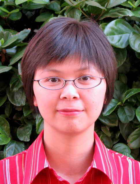 Yu Huang合作论文数Department of Materials Science and Engineering, Henry Samueli School of Engineering and Applied Sciences, University of California Los Angeles1
 Trond Heir合作论文数Norwegian Ctr Violence & Traumat Stress Studies, Oslo, Norway1
 Sriram Madhavan合作论文数1Braun, M.合作论文数1
 Grzegorz Mrugalski合作论文数1
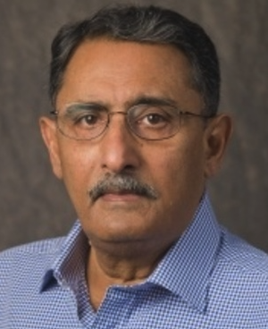 Sudhakar M. Reddy合作论文数Department of Electrical and Computer Engineering, College of Engineering, University of Iowa;Seamans Center for the Engineering Arts and Sciences, University of Iowa1
 Wu-Tung Cheng合作论文数Mentor Graphics1
 Yue Tian合作论文数1Wu Yang合作论文数1
 Nilanjan Mukherjee合作论文数Mentor Graphics Corporation1
 Kun-Han Tsai合作论文数1Rao Desineni合作论文数Carnegie Mellon University1Huaxing Tang合作论文数Mentor Graphics Corporation1Yi-Jung Chang合作论文数1Rob Thompson合作论文数1Randy Klingenberg合作论文数1
 Srikanth Venkataraman合作论文数1Chris Schuermyer合作论文数Logic, LSI1
 Jerzy Tyszer合作论文数Faculty of Computing and Telecommunications, Poznań University of Technology1
 Pankaj Pant合作论文数1Shobhit Malik合作论文数1Nagesh Tamarapalli合作论文数AMD1
 Manish K. Sharma合作论文数AbbVie1mentor graphics合作论文数1
 Ting-Pu Tai合作论文数1
 Dimitris Gizopoulos合作论文数Computer Architecture Laboratory, Department of Informatics and Telecommunications, National and Kapodistrian University of Athens1
 Mark Kassab合作论文数1




