This article gives an overview of our current state of the art in generating 3D geometry and doping representations for complex semiconductor devices. Focusing on the multidimensional aspects, we describe how-starting from the mask layout and the standard process representation (SPR)-the 3D device geometry and doping distribution is built by assembling simulations of different dimensionality.
Designing new semiconductor devices for very large scale integrated circuits (VLSI) requires intensive use of process and device simulation tools to reduce development costs. However, valid device simulation results can only be achieved when a high geometrical modeling precision has been reached during the process simulation phase. Accurate finite element simulators embedded in a multi-dimensional process simulation environment help to fulfill this quality requirement. Since general-purpose three-dimensional (3D) process simulators are not yet available, a modern design environment combines solid modeling techniques with one-dimensional (1D) and two-dimensional (2D) finite element simulators. In this article we present a consistent and integrated process simulation environment that eases the characterization and optimization of semiconductor devices. The straightforward modeling in all three dimensions of an EEPROM cell illustrates the presented approach.
Constructive Solid Geometry (CSG) is a solid modeling technique widely used for the design of semiconductor devices. With the simulation domain subdivision algorithm presented in this paper, the minimal number of solid modeling operations is required in order to build a three-dimensional (3D) device structure. The algorithm is based on a drawing method which combines information on photolithographic masks into a color raster. In this way, solid modeling operations are performed only once on regions having the same color.
Since general-purpose 3D process simulators are currently not available, solid modelers greatly help the designer in building geometries for device simulators. In this contribution, a solid modeler is presented that allows reliable geometrical operations. In order to avoid numerical errors occurring at the intersection of objects built with polygons, we have chosen a data structure based on a discretization of the x-y plane of the simulation domain
We have fabricated 2.5-kV thyristor devices with integrated MOS controlled n+-emitter shorts and a bipolar turn-on gate using a p-channel DMOS technology. Square-cell geometries with pitch variations ranging from 15 to 30-mu-m were implemented in one- and two-dimensional arrays with up to 20 000 units. The impact of the cell pitch on the turn-off performance and the on-state voltage was studied for arrays with constant cathode area as well as for single-cell structures. By realizing MOS components with submicrometer channel lengths, scaled single cells are shown to turn off with current densities of several kiloamperes per square centimeter at a gate bias of 5 V. In the case of multi-cell ensembles, turn-off performance is limited due to inhomogeneous current distribution. Critical process parameters as well as the device behavior were optimized through multi-dimensional numerical simulation.
The authors give an overview of the status of CAD (computer-aided design) tools in power IC design, especially the use of simulation tools and computer-aided layout techniques. They illustrate the possibilities of these tools with two examples from a recent MOS controlled thyristor (MCT) design effort
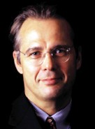 Wolfgang Fichtner合作论文数Department of Information Technology and Electrical Engineering, Eidgenössische Technische Hochschule Zürich6
 Norbert Strecker合作论文数4Josef Burgler合作论文数3h dettmer合作论文数2Heinz Lendenmann合作论文数2T. Feudel合作论文数1norbert strecker合作论文数1stephan muller合作论文数1A Hofler合作论文数1Hofler, Alexander合作论文数1Garreton, G.合作论文数1R. Vuilleumier合作论文数1K. Kells合作论文数1Ernst Halder合作论文数1Peter Roggwiller合作论文数1Friedhelm D. Bauer合作论文数1
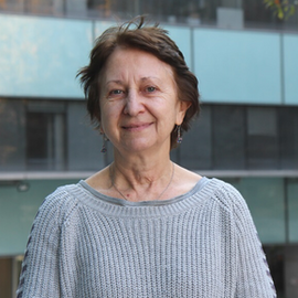 Nancy Hitschfeld合作论文数Departamento de Ciencias de la Computación, Facultad de Ciencias Físicas y Matemáticas, Universidad de Chile1Thomas Feudel合作论文数1
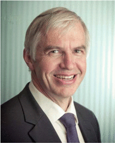 Thomas Stockmeier合作论文数1




