Many proposals to scale quantum technology rely on modular or distributed designs where individual quantum processors, called nodes, are linked together to form one large multinode quantum computer (MNQC). One scalable method to construct an MNQC is using superconducting quantum systems with optical interconnects. However, a limiting factor of these machines will be internode gates, which may be two to three orders of magnitude noisier and slower than local operations. Surmounting the limitations of internode gates will require a range of techniques, including improvements in entanglement generation, the use of entanglement distillation, and optimized software and compilers, and it remains unclear how improvements to these components interact to affect overall system performance, what performance from each is required, or even how to quantify the performance of each. In this paper, we employ a `co-design' inspired approach to quantify overall MNQC performance in terms of hardware models of internode links, entanglement distillation, and local architecture. In the case of superconducting MNQCs with microwave-to-optical links, we uncover a tradeoff between entanglement generation and distillation that threatens to degrade performance. We show how to navigate this tradeoff, lay out how compilers should optimize between local and internode gates, and discuss when noisy quantum links have an advantage over purely classical links. Using these results, we introduce a roadmap for the realization of early MNQCs which illustrates potential improvements to the hardware and software of MNQCs and outlines criteria for evaluating the landscape, from progress in entanglement generation and quantum memory to dedicated algorithms such as distributed quantum phase estimation. While we focus on superconducting devices with optical interconnects, our approach is general across MNQC implementations.
Quantum Communications Networks using the properties of qubits, namely state superposition, no-cloning and entanglement, can enable the exchange of information in a very secure manner across optical links or free space. New innovations enable the use of optical repeaters as well as multi-cast communication in the networks. Some types of quantum communications mechanisms can be implemented at room-temperature instead of requiring super-cooled systems. This makes it likely that business impact from quantum communications will be realized sooner than that from quantum computers. Quantum networks need to be integrated into the ecosystem of currently deployed classical networks and augment them with new capabilities. Classical computers and networks need to be able to use the new secure communication capabilities offered by quantum networks. To provide this interoperability, appropriate software abstractions on the usage of quantum networks need to be developed. In this paper, we examine what the type of software abstractions quantum networks can provide, and the type of applications that the new abstractions can support.
This brief overview of quantum computing gives an intuitive, albeit incomplete view of why it shows promise over any known classical approach to computing. The difficulty of making a qubit which allows us to protect and control quantum information will be illustrated in an overview of existing quantum technologies, including ions, superconducting qubits, spins and defects in solids. Finally, I will review a few of the problems which may benefit most from quantum computing and why many in industry are excited by the prospects.
There has been a good deal of work on algorithms to simulate quantum many-body systems with fault-tolerant quantum computers- those with full error correction. Fault-tolerant quantum computers of scale requisite to achieve computational advantage for these problems are likely over a decade away. Moreover, devices that we can build in the near term, called Noisy Intermediate Scale Quantum computers (NISQ), have too much noise to implement the long circuits required by these algorithms. We review heuristic, short-depth quantum algorithms more suited to NISQ computers; specifically, their scaling properties when applied to electronic and nuclear structure calculations, including Hamiltonian complexity with particle number, ansatz state preparation, convergence, and noise. We will present examples of actual quantum structure calculations with NISQ computers, as well as a newly-developed error mitigation technique that significantly improves accuracy. We end with an outlook for “advantage” – when NISQ systems might excel conventional HPC approaches for comparable problems.
This paper dealts with many qubits technologies being explored; NISQ era today, moving toward FTQC; early demosntration in NISQ algorithms; some practical problem with advantage 3-5 years away; FTQC era with advantage >20 years away.
Submitted for the MAR14 Meeting of The American Physical Society Resistive Switching and Temperature-dependent Transport in HfOx-based Resistive Memory Devices SEYOUNG KIM, IBM T JWatson Research Center, CHIYUI AHN, Stanford University, TAYFUN GOKMEN, OLIVER DIAL, MARK RITTER, IBM T J Watson Research Center — Resistive switching phenomenon in transition metal oxide materials has been studied intensively as a candidate technology for future non-volatile memory applications and electronic synapse devices. Here, we demonstrate an HfOx-based resistive memory device with rare earth metal contact in which the device resistance can be modulated with applied voltage and current. Repeatable and self-compliance switching as well as high yield and device-to-device uniformity are achieved in our devices. To understand the conduction mechanism, we perform transport measurement in multiple devices at different resistance states (initial, low and high resistance states) by probing current as a function of applied voltage at temperatures from 40K to 350K. We find that temperature insensitive tunneling conduction dominates at low temperature, while thermally activated conduction is observed at high temperature. Trap-assisted tunneling and Poole-Frenkel mechanisms are accounted for the characteristics found in different regimes. Seyoung Kim IBM T J Watson Research Center Date submitted: 18 Nov 2013 Electronic form version 1.4
To achieve a target data bandwidth in high-speed channels, an on-board channel modeling study was presented in this paper. A design guideline was found by observing the variation of link performance, depending on parameters such as channel length, baud rate, and the number of signal layers. The channel performance was investigated using a newly developed parametric simulation environment supported by a fast multilayered via transition modeling tool. The extensive parameter sweep simulations showed that an allowable channel reach has a lower and an upper bound limited by stub via effect and trace loss, respectively. Under a specified channel reach, the aggregate data bandwidths were estimated using a particle swarm optimization routine, and a tradeoff relation among the wiring capability and the maximum allowable data rate was observed. From these observations, the approach provides a guideline to select the number of signal layers for achieving the required data bandwidth.
The conduction mechanism of HfOx-based RRAM is investigated by analyzing the I-V characteristics of HfOx-based RRAM devices at different temperatures ranging from 350 K down to 40 K. Electrical conduction of RRAM is found to be strongly dependent on the resistance state of the device, electric field, and temperature. At relatively high electric field (E > 3 MV/cm), Poole-Frenkel conduction explains our measured temperature dependence at limited temperature (T > 200 K) and bias ranges while trap-assisted tunneling accounts for the temperature-insensitive conduction regime (T <; 100 K). It is also concluded that the more resistive RRAM device shows weaker dependence on temperature.
The goal of neuromorphic engineering is to build electronic systems that mimic the ability of the brain to perform fuzzy, fault-tolerant, and stochastic computation, without sacrificing either its space or power efficiency. In this paper, we determine the operating characteristics of novel nanoscale devices that could be used to fabricate such systems. We also compare the performance metrics of a million neuron learning system based on these nanoscale devices with an equivalent implementation that is entirely based on end-of-scaling digital CMOS technology and determine the technology targets to be satisfied by these new devices. We show that neuromorphic systems based on new nanoscale devices can potentially improve density and power consumption by at least a factor of 10, as compared with conventional CMOS implementations.
This article presents a full-wave electromagnetic approach for analyzing the electrical performance of massively coupled through silicon vias (TSV). The TSVs are modeled with SiO(2) insulation coating and are placed in the sandwiched SiO(2)-Si-SiO(2) substrate. The planar guided wave is analyzed to determine the fundamental mode and high order modes in stratified media. Cylindrical wave expansions and Foldy-Lax equations for multiple scattering techniques are adapted to the TSV problems. The effect of SiO(2) coating around the via is modeled by the general expression of T-matrix coefficients. Both dispersive silicon loss and copper loss are included in this approach. Numerical simulation of a 4-by-4 TSV array is demonstrated to show the signal performance and crosstalk. It shows that the coupling issues among the TSVs will become significant beyond 15 GHz. The results are in excellent agreement with general purpose field solver. (C) 2011 Wiley Periodicals, Inc. Microwave Opt Technol Lett 53:1204-1206, 2011; View this article online at wileyonlinelibrary.com. DOI 10.1002/mop.26021
Large, parallel systems have greatly aided scientific computation and data collection, but performance scaling now relies on chip and system-level parallelism. This has happened because power density limits have caused processor frequency growth to stagnate, driving the new multi-core architecture paradigm, which would seem to provide generations of performance increases as transistors scale. However, this paradigm will be constrained by electrical I/O bandwidth limits; first off the processor card, then off the processor module itself. We will present best-estimates of these limits, then show how optical technologies can help provide more bandwidth to allow continued system scaling. We will describe the current status of optical transceiver technology which is already being used to exceed off-board electrical bandwidth limits, then present work on silicon nanophotonic transceivers and 3D integration technologies which, taken together, promise to allow further increases in off-module and off-card bandwidth. Finally, we will show estimated limits of nanophotonic links and discuss breakthroughs that are needed for further progress, and will speculate on whether we will reach Exascale-class machine performance at affordable powers.
Every year, the IBM Research Division undertakes a year-long process to analyze and map out important trends and future directions shaping the advances and the applications of information technology (IT). The results are summarized in a document called the Global Technology Outlook (GTO), which influences IBM's strategy and technology roadmaps. Coinciding with the IBM Centennial, a special chapter was commissioned in the 2011 GTO, which was designed to both reflect on the historical evolution of computers and computation as well as to look a few decades ahead to explore the new frontiers of IT. This paper presents the results of this study. It provides a vision of the future in which advances in technology will enable the creation of a new class of “learning” systems, i.e., designed with people as an integral and central element of the process, and which are explicitly aimed to enhance human cognition. These systems will learn from both structured and unstructured data, find important correlations, create hypotheses for these correlations, and suggest and measure actions to enable better outcomes for users. Systems with these capabilities will transform our view of computers from “calculators” to “machines that learn,” which is a shift that will radically alter our expectations of what computing ought to do for us as humans and that will equip us to successfully navigate the increasing complexity of our globally interconnected world.
Physics-based models for vias and traces including new component models are applied to simulate multilayer interconnects on printed circuit boards. A variety of interconnect structures, including via arrays and differential links between package via fields, are studied with model-to-hardware correlation. These models also enable efficient signal integrity and power integrity co-analysis with focus on modeling simultaneous switching noise coupled into high-speed signal nets as well as understanding the effects of decoupling capacitor placement. Simulation time has been reduced at least three orders of magnitude with respect to comparable full-wave simulations. Author’s Biographies Xiaoxiong Gu received the B.S. degree from Tsinghua University, Beijing, China, in 2000, the M.S. degree from the University of Missouri, Rolla, in 2002, and the Ph.D. degree from the University of Washington, Seattle, in 2006, all in electrical engineering. He is currently a Research Staff Member with the IBM T. J. Watson Research Center. His research interests include characterization of high-speed interconnect and microelectronic packaging, signal integrity and computational electromagnetics. Dr. Gu received the best paper award at ECTC in 2007 and DesignCon Paper Award in 2008. Renato Rimolo-Donadio received the B.S. and Lic. degrees in electrical engineering from the Technical University of Costa Rica (ITCR), Costa Rica, in 1999 and 2004, respectively, and the M.S. degree in microelectronics and microsystems from the Technical University of Hamburg-Harburg (TUHH), Germany, in 2006, where he is currently working toward the Ph.D. degree in electrical engineering. Since November 2006, he has been a Scientific Research Assistant at the Institute of Electromagnetic Theory, Technical University of Hamburg-Harburg. His main research interests include system level modeling and optimization of interconnects, and analysis of signal and power integrity problems at PCB and package level. Francesco de Paulis received his Laurea degree and his Specialistic degree (summa cum laude) in Electronic Engineering from University of L’Aquila, L’Aquila, Italy, in 2003 and 2006, respectively. He was involved in the research activities of the UAq EMC Laboratory from August 2004 to August 2006. From June 2004 to June 2005 he had an internship at Selex Communications s.p.a. within the layout/SI/PI design group. In August 2006 he joined the EMC Laboratory at the Missouri University of Science and Technology (formerly University of Missouri-Rolla), where he pursued a Master of Science Degree in Electrical Engineering in May 2008. He is currently enrolled in PhD program at the University of L’Aquila, L’Aquila, Italy. His main research interests are in developing fast and efficient analysis tool for SI/PI design of high speed signal on PCB, RF interference in mixed-signal system, EMI problem investigation on PCBs. Zhenwei Yu received his B.S. degree in Mathematics and Physics, and M.S. degree in Electrical Engineering from Tsinghua University, Beijing, China, in 2005 and 2007 respectively. Currently he is a Ph.D. candidate with the EMC Laboratory at Missouri University of Science and Technology (formerly University of Missouri-Rolla). His research interests include modeling of IC emissions, RF interference, PCB noise mitigation, and tool development for Signal Integrity and Electromagnetic Compatibility designs in high-speed PCBs. He was a Co-op at IBM, Research Triangle Park, NC, from January to July 2009 and worked in the EMC modeling tool development. Young H. Kwark received his BSEE from the Massachusetts Institute of Technology and his MSEE/PhD from Stanford University. His work experience as a Research Staff Member at the IBM T. J. Watson Research Center, Yorktown Heights, NY, includes circuit design for optical links and wireless applications. He is currently involved in package characterization for high performance computing platforms. Dr. Kwark received DesignCon Paper Awards in 2005, 2006 and 2008. Matteo Cocchini received his Laurea (5-year degree) in Electronic Engineering in June 2006 from University of L'Aquila, L'Aquila, Italy, where he got involved in the research activities of the UAq EMC Laboratory in 2005 and 2006. In August 2006, he joined the MST EMC Lab at the Missouri University of Science and Technology, where his research activity included via transition modeling and power distribution network simulations. He got a Master of Science in Electrical Engineering from the same University in May 2008. He currently works as Signal and Power Integrity Engineer for the IBM I/O packaging and development team in Poughkeepsie, New York. Mark B. Ritter received a B.S. degree in physics from Montana State University in 1981 and M.S., M.Phil. and Ph.D. degrees in Applied Physics from Yale University in 1987. His work at IBM has focused on high-speed I/O circuit and package design, with work including Fibre Channel, 10 Gb/s Ethernet, and 40 Gb/s analog front end circuits as well as interconnect structures for high-speed data transmission. Dr. Ritter presently manages a group focusing on high-speed I/O subsystems. Dr. Ritter was the recipient of the 1982 American Physical Society Apker Award and DesignCon Paper Award in 2008. Bruce Archambeault is a Senior Technical Staff Member at IBM in Research Triangle Park, NC. He received his B.S.E.E degree from the University of New Hampshire in 1977 and his M.S.E.E degree from Northeastern University in 1981. He received his Ph. D. from the University of New Hampshire in 1997. Dr. Archambeault has authored or co-authored a number of papers in computational electromagnetics, mostly applied to real-world EMC applications. He is currently a member of the Board of Directors for the IEEE EMC Society and a past Board of Directors member for the Applied Computational Electromagnetics Society (ACES). He has served as a past IEEE/EMCS Distinguished Lecturer and Associate Editor for the IEEE Transactions on Electromagnetic Compatibility. Albert E. Ruehli received his Ph.D. degree in Electrical Engineering in 1972 from the University of Vermont, and an honorary Doctorate in 2007 from the Lulea University in Sweden. He has been a member of various projects with IBM including interconnect tools and modeling and manager of both a VLSI design and CAD group. From 1972 to 2009, he was with IBM’s T.J. Watson Research Center. Currently, he is an Adjunct Professor at the Missouri University of S&T and an Emeritus at IBM. He is the editor of two books and author or coauthor of over 180 technical papers. He received five IBM Awards, the Guillemin-Cauer Prize in 1982, and the Golden Jubilee Medal from the IEEE CAS Society in 1999. He received a Certificate of Achievement from the IEEE EMC society in 2001, the 2005 Richard R Stoddart Award, and in 2007 he received the Honor ary Life Member Award from the IEEE EMC Society and is a Life Fellow of the IEEE and a member of SIAM. Jun Fan received his B.S. and M.S. degrees in Electrical Engineering from Tsinghua University, Beijing, China, in 1994 and 1997, respectively. He received his Ph.D. degree in Electrical Engineering from the University of Missouri-Rolla in 2000. From 2000 to 2007, he worked for NCR Corporation, San Diego, CA, as a Consultant Engineer. In July 2007, he joined the Missouri University of Science and Technology (formerly University of Missouri-Rolla), and is currently an Assistant Professor with the UMR/MS&T EMC Laboratory. His research interests include signal integrity and EMI designs in high-speed digital systems, dc power-bus modeling, intra-system EMI and RF interference, PCB noise reduction, differential signaling, and cable/connector designs. Dr. Fan serves as the Chair of the TC-9 Computational Electromagnetics Committee, the Secretary of the Technical Advisory Committee, and a Distinguished Lecturer of the IEEE EMC Society. Christian Schuster received the Diploma degree in physics from the University of Konstanz, Germany, in 1996, and the Ph. D. degree in electrical engineering from the Swiss Federal Institute of Technology (ETH), Zurich, Switzerland, in 2000. From 2001 to 2006 he was a Research Staff Member at the IBM T. J. Watson Research Center, Yorktown Heights, NY. Since October 2006, Dr. Schuster is a full professor of electrical engineering at the Technische Universität Hamburg-Harburg (TUHH), Germany. Dr. Schuster received DesignCon Paper Awards in 2005 and 2006. He is a senior member of the IEEE.
This paper introduces an efficient environment for parametric and statistical studies of electrical link performance. With this simulation environment and its use of systematic input and output files, the effects of both physical and electrical design parameters can be readily observed. In addition, supported by fast electromagnetic and link simulators, the environment enables the extensive studies of electrical links by considering the effects of changing many design parameters. An exemplary parametric study in this paper shows the usefulness of the simulation environment for various future applications.
 Young-Je Kwark合作论文数Department of Organic Materials and Fiber Engineering, Soongsil University16
 Kevin Gu合作论文数IBM T. J. Watson Research Center13
 Christian Schuster合作论文数Institut für Theoretische Elektrotechnik, School of Electrical Engineering, Computer Science, and Mathematics, Hamburg University of Technology;Lothar Collatz Center for Computing in Science, University of Hamburg10
 Lei Shan合作论文数8
 Christian Baks合作论文数6
 Daniel M. Kuchta合作论文数IBM T. J. Watson Research Center6
 Renato Rimolo-Donadio合作论文数Rydev Inc.;Tecnológico de Costa Rica6
 Petar K. Pepeljugoski合作论文数IBM Thomas J. Watson Research Center6jeannine m trewhella合作论文数5Rogers, D.合作论文数5
 Fuad E. Doany合作论文数Thomas J. Watson Research Center, IBM Research5
 Albert Ruehli合作论文数EMC Laboratory, Missouri University of Science and Technology5Jeffrey A. Kash合作论文数Center for Integrated Science and Engineering, Columbia University5r k puri合作论文数4Philip G. Emma合作论文数4modest m oprysko合作论文数4
 Seyoung Kim合作论文数Pohang Univ Sci & Technol POSTECH, Dept Mat Sci & Engn, Pohang 37673, South Korea4
 Daniel J. Friedman合作论文数National Renewable Energy Laboratory4
 Kerry Bernstein合作论文数Modern Technology Solutions, Inc.4Jeannine M Trewhella合作论文数4
 Paul W. Coteus合作论文数4
 Boping Wu合作论文数4raymond robert horton合作论文数3peter g ledermann合作论文数3
 Lawrence Jacobowitz合作论文数3glen w johnson合作论文数3albert m young合作论文数3daniel j stigliani合作论文数3Bregman, M.F.合作论文数3D. Rogers合作论文数3
 Clint Schow合作论文数Department of Electrical and Computer Engineering, College of Engineering, University of California Santa Barbara3
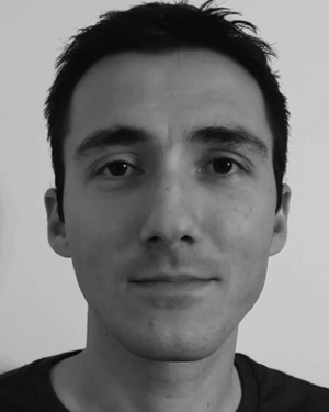 Tayfun Gokmen合作论文数Department of Electrical Engineering;Princeton University;Department of Electrical Engineering, Princeton University3Alphonso P. Lanzetta合作论文数3Richard A. John合作论文数3Bruce Archambeault合作论文数Missouri University of Science and Technology3
 Ibrahim Elfadel合作论文数Masdar Institute, Khalifa University;Center for Cyber-Physical Systems, Khalifa University;Laboos Technologies3
 Giuseppe Selli合作论文数3
 Sudhir M. Gowda合作论文数THOMAS J WATSON RES CTR, IBM CORP3i c noyan合作论文数2dennis l karst合作论文数2michael j palmer合作论文数2
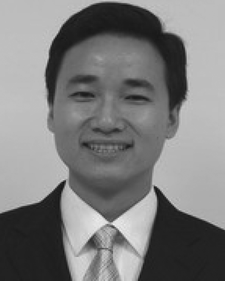 zhenwei yu合作论文数2ismail cevdet noyan合作论文数2
 Francesco de Paulis合作论文数UAq EMC Laboratory, University of L'Aquila2
 Matteo Cocchini合作论文数2
 Oliver E Dial合作论文数Massachusetts Institute of Technology2
 Ethan C. Ahn合作论文数2Kam, D.合作论文数2Cina, M.F.合作论文数2




