A summary of contributions made by significant papers from the first 25 years of the Field-Programmable Logic and Applications conference (FPL) is presented. The 27 papers chosen represent those which have most strongly influenced theory and practice in the field.
New Algorithms, Architectures and Applications for Reconfigurable Computing consists of a collection of contributions from the authors of some of the best papers from the Field Programmable Logic conference (FPL03) and the Design and Test Europe conference (DATE03). In all, seventy-nine authors, from research teams from all over the world, were invited to present their latest research in the extended format permitted by this special volume. The result is a valuable book that is a unique record of the state of the art in research into field programmable logic and reconfigurable computing. The contributions are organized into twenty-four chapters and are grouped into three main categories: architectures, tools and applications. Within these three broad areas the most strongly represented themes are coarse-grained architectures; dynamically reconfigurable and multi-context architectures; tools for coarse-grained and reconfigurable architectures; networking, security and encryption applications. Field programmable logic and reconfigurable computing are exciting research disciplines that span the traditional boundaries of electronic engineering and computer science. When the skills of both research communities are combined to address the challenges of a single research discipline they serve as a catalyst for innovative research. The work reported in the chapters of this book captures that spirit of that innovation.
Interfacial interactions at graphene/metal and graphene/dielectric interfaces are likely to profoundly influence the electronic structure of graphene. We present here the first angle-resolved near-edge X-ray absorption fine structure (NEXAFS) spectroscopy study of single- and bilayered graphene grown by chemical vapor deposition on Cu and Ni substrates. The spectra indicate the presence of new electronic states in the conduction band derived from hybridization of the C-pi network with Cu and Ni d-orbitals. In conjunction with Raman data demonstrating charge transfer, the NEXAFS data illustrate that the uniquely accessible interfaces of two-dimensional graphene are significantly perturbed by surface Coatings and the underlying substrate. NEXAFS data have also been acquired after transfer of graphene onto SiO2/Si substrates and indicate that substantial surface corrugation and misalignment of graphene is induced during the transfer process. The rippling and corrugation of graphene, studied here by NEXAFS spectroscopy, is thought to deleteriously impact electrical transport in graphene.
A review of literature combined with recent experimental results addressing the intrinsic and extrinsic factors controlling the effective work function (EWF) of metal gate electrodes on Hf-based high-K dielectrics is discussed. Through a systematic study including accurate extraction of EWF, our observations suggest, unlike popularly perceived, intrinsic Ef-pinning does not limit the EWF tuning on high-K. Also, a critical issue challenging the maintenance of high EWF metals at low effective oxide thicknesses (EOT), due to a new phenomena described as the "Vfb roll-off", is reported for the first time.
Summary form only given.FPGAs are the most successful example to date of programmable concurrent architectures. The 1980s saw the introduction of several kinds of concurrent processing arrays, ranging from fine-grained FPGAs to systolic arrays, to arrays of microprocessors. Of these, only FPGAs have enjoyed continuous commercial success. Now, however, with the end of the four-decade-old trend towards faster microprocessors, we are witnessing the revival of processor arrays. Due largely to concerns about power consumption multi-core, and indeed many-core architectures, are back at the forefront of system design. It is clear that we have the silicon resources and the circuit design skills to deliver semiconductor devices with highly concurrent programmable architectures and that the aggregate compute power of these arrays is impressive. What is not so straightforward is whether we now have the methodologies and automated tools to efficiently design systems of the complexity demanded by current and future markets. For example, we might enquire whether almost forty years of experience with microprocessors has made us any better prepared for the revival of many-core architectures. Paradoxically, the success of the uni-processor programming model may be the most significant impediment to our future success with highly concurrent, programmable architectures. Or taking an alternative perspective, we might ask whether we can benefit from over 25 years of experience of successfully deploying the programmable concurrency of FPGAs. In this talk, we will re-visit the challenges posed by programmable concurrent architectures and explore some of the assumptions underlying them in an effort to assess the potential of emergent solutions.
A series of 1.4, 1.8, and 4.0nm thick HfO2 films deposited on Si(100) substrates have been measured by extended X-ray absorption fine-structure prior to anneal processing, following a standard post deposition anneal of 700°C for 60s in NH3 ambient, and following an additional rapid thermal anneal cycle of 1000°C for 10s in N2 ambient. Analysis of the second coordination shell gives clear evidence of increased ordering with increasing film thickness at each temperature. Similarly, increased ordering with increasing anneal temperature is evident for each film thickness. Although X-ray diffraction and high resolution transmission electron microscopy indicated the 1.4nm HfO2 samples to be amorphous, EXAFS has distinguished nanocrystalline from amorphous states for these films.
This work investigates the capability of spectroscopic ellipsometry to measure charge trapping centers in thin dielectric films. Specific interfacial electrostatic fields, induced by electrons injected into charge trapping states at the interface, have been identified that directly affect the underlying silicon substrate critical points. The effect of a field-induced change in the silicon fundamental absorption edge due to different processing conditions affecting the oxygen vacancy defects at the interface is presented. Measuring the field-induced change in the silicon dielectric function between a sample with a 2 nm WO, film as-deposited and the same sample after a 1000 degrees C anneal in an N-2 ambient reveals that a stronger interfacial field is present for the as-deposited HfO2 film. These results are consistent with the understanding that high temperature anneals work well to passivate oxygen vacancy defects at the silicon/HfO2 interface. Finally, we compare our results with Second Harmonic Generation where specific resonant features are identifiable with electric field enhancements at the same interface. (C) 2008 WILEY-VCH Verlag GmbH & Co. KGaA, Weinheim.
HfO2 gate dielectric thin films have been exposed to anneal processing in NH3 and N2 ambient in order to decouple the influence of N incorporation from that of the thermal cycle alone. We report on the effectiveness of NH3 processing to introduce N into the dielectric film system during intermediate temperature annealing. Several high‐resolution techniques including electron microscopy with electron energy loss spectra (EELS), rotationally averaged selective area electron diffraction, grazing incidence X‐ray diffraction and synchrotron X‐ray photoelectron spectroscopy (XPS) have been utilized to elucidate chemical composition and crystalline structure differences between samples annealed in NH3 and N2 ambient as a function of temperature. Copyright © 2006 John Wiley & Sons, Ltd.
 Gordon McGregor合作论文数Freescale Semiconductor10
 David Robinson合作论文数10Brandon Blodget合作论文数6Adam Donlin合作论文数 Department of Computer Science here at Edinburgh University6B. Foran合作论文数4Hugh Dick合作论文数4Jon Stockwood合作论文数4
 Gennadi Bersuker合作论文数Aerospace Corporation4
 Stephen Marshall合作论文数Department of Electronic and Electrical Engineering, University of Strathclyde3Neil Woolfries合作论文数3Raj Jammy合作论文数3
 James Irvine合作论文数University of Strathclyde3B. Blodget合作论文数2paul m hartke合作论文数2seungchul song合作论文数2HR Huff合作论文数2John Dunlop合作论文数2
 Stemmer Susanne合作论文数Departmrnt of Materials, College of Engineering, University of California, Santa Barbara2
 Lee, Byoung Hun合作论文数Department of Electrical Engineering, Pohang University of Science and Technology;Exploratory Electronic System Laboratory, Pohang University of Science and Technology2Ian Robertson合作论文数2
 Hayden Kwok-Hay So合作论文数Department of Electrical and Electronic Engineering,The University of Hong Kong2John Macbeth合作论文数2
 Reiner W. Hartenstein合作论文数Kaiserslautern University of Technology, CS dept2
 Oliver Diessel合作论文数School of Computer Science & Engineering, Faculty of Engineering, The University of New South Wales2Delon Levi合作论文数2
 Marco Platzner合作论文数Department of Computer Engineering, Faculty for Electrical Engineering, Computer Science, and Mathematics, Paderborn University2Roy Chapman合作论文数1bernard pottier合作论文数1
 JJ Peterson合作论文数1Viorel Onofrei合作论文数1
 Qingkai Yu (于庆凯)合作论文数Shanghai Institute of Microsystem and Information Technology, Chinese Academy of Sciences;University of Chinese Academy of Sciences1Zhiqiang Chen合作论文数1michael dales合作论文数1Chanro Park合作论文数1j r taylor合作论文数1y q an合作论文数1
 Tobias Becker合作论文数Department of Computing, Faculty of Engineering, Imperial College London1
 Philip Leong (梁恆惠)合作论文数Faculty of Engineering, The University of Sydney;Computer Engineering Laboratory, School of Electrical and Information Engineering, The University of Sydney;ClusterTech Limited1Sedcole, P.合作论文数1
 Casey Smith合作论文数sematech1John Gisby合作论文数1Mason, J.合作论文数1Hiroaki Niimi合作论文数1
 Husam Alshareef合作论文数Physical Science and Engineering Division, King Abdullah University of Science and Technology1
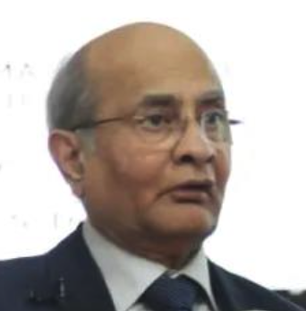 Tariq Salim Durrani (塔里克·杜拉尼)合作论文数University of Strathclyde Glasgow1
 Mark Shand合作论文数1
 P. A. Subrahmanyam合作论文数1
 Joseph Woicik合作论文数Ceramics Division, National Institute of Standards and Technology1
 Hideharu Amano (天野英晴)合作论文数Department of Information and Computer Science, Faculty of Science and Technology, Keio University1




