This article describes a defect-oriented test (DOT) approach, which enables a complete physical defect-based automatic test pattern generation (ATPG) for the digital logic area of CMOS-based designs. Total critical area (TCA)-based methods are presented for the generation of needed DOT views to enable the generation of complete DOT-based patterns for detecting all cell-internal and as well all cell-external physical defects. The major aim of these new methods and patterns is to further reduce the defect rate of manufactured ICs, in addition to what is already achieved with traditional and cell-aware test (CAT) fault models. We present test results, including achieved defect rate reduction in defective parts per million (DPPM), from a large 14-nm FinFET design, including a correlation to system-level-test (SLT) fails. For a second, mature 160-nm automotive mixed-signal sensor we present high-volume production test results, again measured in DPPM, and we provide test coverage figures moving away from counting detected faults to calculating detected TCA which is reported as the chip level TCA coverage.
The European Test Symposium (ETS) Best Paper Award, which was introduced in 2004 when the European Test Workshop (ETW) turned into the ETS, aims to maintain and encourage the high quality of papers and presentations in the ETS technical program. Eligible for the ETS Best Paper Award are papers published in the Formal Proceedings of ETS and presented in a full-length oral presentation slot in the regular technical program. The Best Paper is selected by the Best Paper Selection Committee (BPSC), appointed by the Program Committee, taking into account the inputs from reviewers, Topic Chairs and symposium attendees. Based on these inputs, the BPSC recommended the paper to be awarded and the final decision was taken by the Program Committee. It is our pleasure to announce that the Best Paper Award of ETS'19 goes to the paper entitled: "Digital Built-in Self-Test for Phased Locked Loops to Enable Fault Detection" by Mehmet INCE, Sule OZEV (Arizona State University, AZ, USA). The award is formally handed over during the plenary opening session of ETS'20.
This paper presents new methods and experimental production test results from completely moving away from traditional fault methods towards using critical area based methods instead. The focus of this paper is on measuring the quality of test patterns not by measuring the test coverage but by measuring the covered or detected total critical area (TCA). This is the first time that a TCA for all defects in the digital logic part of a chip can be calculated. The paper will present TCA figures from defect extraction on interconnects outside of standard cells as well as for all defects inside standard cells. We also will present methods for extracting cell-neighborhood defects, their TCA and which of those defects are not covered by cell-aware and interconnect test patterns.
This chapter describes that the works to address tests of small-delay defects have focused on enhancing transition fault tests. Generation of such tests requires the automatic test pattern generation tool to be aware of the circuit delays. The application of a test pattern at a higher clock speed reduces the available system slack on all paths, thereby increasing the chances of detection of small-delay defects on all paths. Because traditional delay test methods target relatively large defects, including a more thorough coverage of small-delay defects can lead to significant improvements in quality levels. The test objective is to screen defective parts from manufactured devices. Defects could modify the functionality or performance of devices. Defects are physical and thus are not amenable to analysis by taking advantage of Boolean algebra used to design and analyze digital logic circuits. To facilitate analysis of defects and the derivation of tests, fault models are used to model defects.
Stringent quality requirements in the automotive sector result in the necessity of targeting additional fault models beyond traditional stuck-at and transition. This paper is concerned with bridging faults, which are well known to require additional tests to detect those which are not detected by traditional tests. To keep ATPG tractable, bridging faults must be extracted from layout to obtain nodes which are physically close together. There are well established methods for such extraction but typically involve complex flows with several tools. This paper describes a much simpler approach using the same layout database that is used for layout-aware diagnosis. The extraction process automatically ranks bridges on critical area so it is simple to truncate the fault list, if necessary. Since each bridge has a critical area it is also possible to provide a weighted critical area based coverage, which is physically more realistic than a simple fault count. The paper describes experimental results, including coverage gains, critical area calculation, and explores physical versus traditional coverage metrics.
Volume diagnosis of scan fails is au effective method of identifying dominant defect mechanisms for yield improvement. However, traditional diagnosis is at the library cell level and identifies only interconnect defects and defective cells. In practice, many defects affect only the internal logic of cells, such as polysilicon contacts, but cannot be pinpointed, resulting in not identifying some potential yield limiters. This paper describes a solution to the problem by showing how diagnosis can be extended to internal cell defects. This is enabled by characterizing a cell library similar to what is needed for cell-aware ATPG, but including more information for diagnosis such as layout data. A flow is described to produce the characterization, which includes requirements for the cell views. Diagnosis results include layout marker files for cell internal suspects which can be viewed in a GDS newer and used to obtain X/Y coordinates to guide physical failure analysis. Successful implementation is demonstrated for a 160nm automotive product.
The European Test Symposium (ETS) Best Paper Award, which was introduced in 2004 when the European Test Workshop (ETW) turned into the ETS, aims to maintain and encourage the quality of papers and presentations in the ETS technical program.
Each year, VTS proudly presents the Best Paper Award to the author(s) of the most outstanding paper from those presented at the previous year's symposium. The candidates for this honor are initially selected based solely on the numerical ratings of the reviewers and symposium attendees, as recorded on the review forms and the session rating cards. The Best Paper Award Judges then carefully review the candidate papers as published in the proceedings. The judges provide numerical scores and comments for each candidate paper. The scores and comments are compiled to select the best paper.
Increasing process variations result in increasing statistical diversity in manufactured devices. Test plans that are developed without this diversity in mind are bound to result in poor test quality/yield and/or long test times. Adaptive testing is a general term that is used to tailor the test strategy to accommodate a wide range of variation in the statistical characteristics of manufactured devices. In this paper, we provide a review of the key works in both digital and analog domains.
This article describes the development of adaptive testing in response to the ever-growing need to dynamically and cost-effectively tailor IC testing to discriminately manage manufacturing process variations. Various degrees of adoption are presented, together with benefits and examples of its use. Finally, challenges for future development are discussed.
Nanoelectronic circuits are increasingly affected by massive statistical process variations, leading to a paradigm shift in both design and test area. In circuit and system design, a broad class of methods for robustness like statistical design and self calibration has emerged and is increasingly used by the industry. The test community's answer to the massive-variation challenge is currently adaptive test. The test stimuli are modified on the fly (during test application) based on the circuit responses observed. The collected circuit outputs undergo statistical post-processing to facilitate pass/fail classification. We will present fundamentals of adaptive and robust test techniques and their theoretical background. While adaptive test is effective, the understanding how it covers defects under different process parameter combinations is not fully established yet with respect to algorithmic foundations. For this reason, novel analytic and algorithmic approaches in the field of variation-aware testing will also be presented in the tutorial. Coverage of defects in the process parameter space is modeled and maximized by an interplay between special fault simulation and multi-constrained ATPG algorithms. These systematic approaches can complement adaptive test application schemes to form a closed-loop system that combines analytical data with measurement results for maximal test quality.
This paper describes the development of adaptive test in response to the ever growing need to dynamically and cost effectively tailor IC testing to discriminately manage manufacturing process variations. Various degrees of adoption are presented, together with benefits and examples of it's use. Finally, challenges for future development are discussed.
This tutorial discusses test methods and voltage stress approaches required to ensure effective cost effective defect screening to produce high quality, reliable products. Wafer level reliability screens (WLRS) refers to the application of screens during wafer test that will both activate and detect a sufficient number of defects so that early life failure rate (ELFR) is reduced enough to meet customer spec, preferably without doing burn-in. Further, these screens have to have acceptable yield loss and acceptable test times.
This paper describes several different approaches to obtain test cost reduction, with emphasis on experimental results obtained for a class of ASICs, although the techniques are general. A review is given of some architectural approaches before giving details of techniques which address reduction in test time. The importance of the gathering and analysis of production data is highlighted with a view to better balance wafer and package tests, eliminate ineffective tests, truncate existing tests and carefully examine at which voltage a test should be run. Stress testing is also discussed with the goal of optimizing tests which are run before and after stress.
We have implemented in Python the COmparative GENomic Toolkit, a fully integrated and thoroughly tested framework for novel probabilistic analyses of biological sequences, devising workflows, and generating publication quality graphics. PyCogent includes connectors to remote databases, built-in generalized probabilistic techniques for working with biological sequences, and controllers for third-party applications. The toolkit takes advantage of parallel architectures and runs on a range of hardware and operating systems, and is available under the general public license from http://sourceforge.net/projects/pycogent .
Complex systems of interactions govern, the structure and function of biomolecules. Mutations that substantially disrupt these interactions are deleterious and should not persist under selection. Yet, several instances have been reported where a variant confirmed as pathogenic in one species is fixed in the orthologs of other species. Here we introduce a novel method for detecting compensatory substitutions for these so-called compensated pathogenic deviations (CPDs), incorporating knowledge of pathogenic variants into a probabilistic method for detecting correlated evolution. The success of this approach is demonstrated for 26 of 31 CPDs observed in mitochondrial transfer RNAs and for one in beta hemoglobin. The detection of multiple compensatory sites is demonstrated for two of these CPDs. The methodology is applicable to comparative sequence data for biomolecules expressed in any alphabet, real or abstract. It provides a widely applicable approach to the prediction of compensatory substitutions for CPDs, avoiding any reliance on rigid non-probabilistic criteria or structural data. The detection of compensatory substitutions that facilitate the substitution of otherwise pathogenic variants offers valuable insight into the molecular constraints imposed on adaptive evolution.
BACKGROUND:Phylogenetic footprinting is the identification of functional regions of DNA by their evolutionary conservation. This is achieved by comparing orthologous regions from multiple species and identifying the DNA regions that have diverged less than neutral DNA. Vestige is a phylogenetic footprinting package built on the PyEvolve toolkit that uses probabilistic molecular evolutionary modelling to represent aspects of sequence evolution, including the conventional divergence measure employed by other footprinting approaches. In addition to measuring the divergence, Vestige allows the expansion of the definition of a phylogenetic footprint to include variation in the distribution of any molecular evolutionary processes. This is achieved by displaying the distribution of model parameters that represent partitions of molecular evolutionary substitutions. Examination of the spatial incidence of these effects across regions of the genome can identify DNA segments that differ in the nature of the evolutionary process.RESULTS:Vestige was applied to a reference dataset of the SCL locus from four species and provided clear identification of the known conserved regions in this dataset. To demonstrate the flexibility to use diverse models of molecular evolution and dissect the nature of the evolutionary process Vestige was used to footprint the Ka/Ks ratio in primate BRCA1 with a codon model of evolution. Two regions of putative adaptive evolution were identified illustrating the ability of Vestige to represent the spatial distribution of distinct molecular evolutionary processes.CONCLUSION:Vestige provides a flexible, open platform for phylogenetic footprinting. Underpinned by the PyEvolve toolkit, Vestige provides a framework for visualising the signatures of evolutionary processes across the genome of numerous organisms simultaneously. By exploiting the maximum-likelihood statistical framework, the complex interplay between mutational processes, DNA repair and selection can be evaluated both spatially (along a sequence alignment) and temporally (for each branch of the tree) providing visual indicators to the attributes and functions of DNA sequences.
Summary form only given. Low cost CMOS image sensors are used in various applications, but the most prominent are camera phones, the fastest growing consumer electronics product in history, going mainstream in less than 5 years from initial introduction. The use of CMOS rather than CCD is discussed, and circuit details given of common pixel designs. The more recent four transistor cell is compared with three transistor cells with respect to image quality and noise. Necessary enhancements to a traditional CMOS process are discussed, needed to produce color filters over individual pixels and a microlens array to capture more light. An integral part of typical systems is an image processor, which takes raw sensor data and converts it into a color image. Brief details of a typical image pipeline are presented, which includes descriptions of demosaic, white balance, color correction and gamma correction. Test considerations deal primarily with the sensor array. The image pipeline is digital logic and tested using traditional approaches. Although these are primarily structural, the dedicated nature of the logic allows some functional tests to be used as effective screeners. Wafer test of digital logic must have high coverage as scan based tests are typically not able to be applied at module level. Array defects can give rise to either random or fixed pattern noise. The eye is significantly more sensitive to fixed pattern noise so special effort is needed to detect it. Causes of defects are discussed, breaking them down into silicon defects and fall-on particles. It is shown how manifestation of these defects, as image blemishes, varies considerably according to test conditions. These conditions include illumination level, exposure, temperature, and whether raw sensor images or demosaiced color images are analyzed. Defective pixel cluster size and amount of deviance are also parameters which need to be considered. Finally, pixel correction is discussed. Since the sensor is a large array, spatial redundancy is utilized to correct isolated defective pixels based on values of neighbor pixels. The challenge is to avoid classifying good pixels as bad, which results in replacing their values, thereby corrupting an otherwise perfectly good image.
 Robert Aitken合作论文数ARM10
 W. Needham合作论文数5
 Hans-Joachim Wunderlich合作论文数Institute of Computer Architecture and Computer Engineering, Universitat Stuttgart4
 Friedrich Hapke合作论文数4
 Robert Saint合作论文数Coll Med & Publ Hlth, Finders Univ3
 Sudhakar M. Reddy合作论文数Department of Electrical and Computer Engineering, College of Engineering, University of Iowa;Seamans Center for the Engineering Arts and Sciences, University of Iowa3
 Sybille Hellebrand合作论文数University of Innsbruck;Institute of Electrical Engineering and Information Technology, University of Paderborn3Eldon E. Ball合作论文数Research School of Biological Sciences, Australian National University3
 Phil Nigh合作论文数Broadcom Inc.3
 Gavin A. Huttley合作论文数Centre for Bioinformation Science;John Curtin School of Medical Research and Mathematical Sciences Institute;Australian National University;John Curtin School of Medical Research and Mathematical Sciences Institute, Australian National University3
 Stephen Rudd合作论文数Buchanan Staffing Group3Ulrich Technau合作论文数3
 Michel Renovell合作论文数Laboratory of Informatics, Robotics and Microelectronics of Montpellier3Lauretta C. Grasso合作论文数3
 Hans G. Kerkhoff合作论文数university of twente3P. W. Baker合作论文数3David C. Hayward合作论文数Centre for the Molecular Genetics of Development and Research School of Biological Sciences, Australian National University3Rc Aitken合作论文数2Haruo Kobayashi合作论文数2T.W. Holstein合作论文数2Jerzy Dabrowski合作论文数2Nicola Nicolici合作论文数2Kai-Chiang Wu合作论文数2Osman Ekekon合作论文数2karen lee bentz合作论文数2Jin-Fu Li合作论文数2Hans A. R. Manhaeve合作论文数2
 Kanad Basu合作论文数Department of Electrical & Computer Engineering, University of Texas at Dallas2
 Ozgur Sinanoglu合作论文数Department of Electrical and Computer Engineering, Tandon School of Engineering, New York University Abu Dhabi2
 Leendert Huisman合作论文数2
 David J. Miller合作论文数Department of Animal Sciences, Education and Communications, College of Agricultural, Consumer and Environmental Sciences, University of Illinois at Urbana-Champaign2
 Krishnendu Chakrabarty合作论文数School of Electrical, Computer and Energy Engineering, Arizona State University;University of Bremen2
 Salvador Mir合作论文数TIMA Laboratory, CNRS-Grenoble INP-UJF),2
 Mihalis Psarakis合作论文数University of Piraeus2
 Ioannis Voyiatzis合作论文数Department of Informatics, Technological Educational Institute of Athens2
 Christoph W. Sensen合作论文数Hungarian Centre of Excellence for Molecular Medicine2
 Luis Entrena合作论文数Electronic Technology Department, Universidad Carlos III de Madrid2
 Eduardo Bezerra合作论文数2Charles F. Hawkins合作论文数2
 Shyue-Kung Lu合作论文数2
 Patrick GIRARD合作论文数Microelectronics Department, Laboratory of Informatics, Robotics and Microelectronics of Montpellier;French National Center for Scientific Research2
 Subhasish Mitra合作论文数Department of Electrical Engineering, Stanford University;Department of Computer Science, Stanford University2
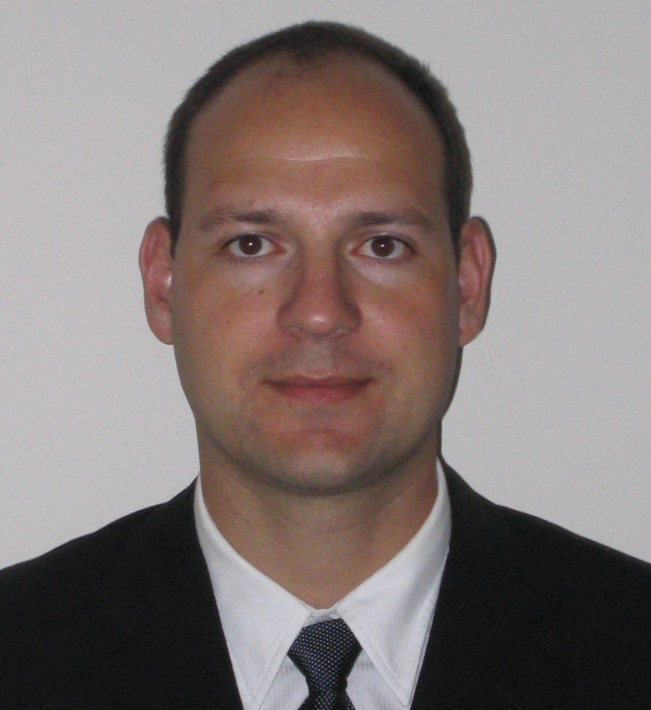 Yiorgos Makris合作论文数Trusted and RELiable Architectures Laboratory, Department of Electrical and Computer Engineering, Erik Jonsson School of Engineering & Computer Science, The University of Texas at Dallas2Vic Johansen合作论文数2Michele Favalli合作论文数Computer Science;University of Ferrara2
 Nur A. Touba合作论文数Chandra Department of Electrical and Computer Engineering, Cockrell School of Engineering, The University of Texas at Austin;Computer Engineering Research Center, University of Texas at Austin2Michael Saina合作论文数2
 Hao-Chiao Hong合作论文数Dept Elect & Comp Engn, Natl Chiao Tung Univ2




