The future upgrading to raster scanning mode in the beam delivery system of Shanghai Advance Proton Therapy facility, pushes the performance of global intensity flatness into the essential requirement, in that dose distribution is sensitive to beam intensity fluctuations. The combination of feedforward and feedback method, by means of implementing the sum of feedforward and feedback outputs as the amplitude of transverse RF field in kicker, is employed in the global intensity control system. The fixed AM function, independent of reference intensity, is used in the feedforward method. The ionization chamber is used as intensity sensor in the feedback method. How to satisfy the global spill flatness with arbitrary reference intensity in large dynamic range is studied in this paper. The experimental results are also presented, in which less than 10% global intensity flatness could be achieved with arbitrary reference intensity in 10 times range.
Magnetic resonance (MR) imaging is a noninvasive, nonionizing clinical modality widely used to detect and visualize anatomical and pathological conditions, including cancer. However, its effectiveness is often limited by low intrinsic sensitivity, insufficient targeting specificity, and poor contrast between normal and tumor tissues. Inspired by the natural use of multivalent interactions in biological adhesion, recognition, and signaling, we report a dual-multivalent enhancement strategy for designing a tetra-armed macrocyclic gadolinium(III)-based molecular MR contrast agent (GdCAG). This agent incorporates four carboxylic alkyl arms and four glucosyl targeting ligands, enabling simultaneous relaxivity enhancement and tumor-selective recognition. GdCAG exhibits significantly improved MR relaxivity as well as markedly enhanced tumor affinity, resulting in effective in vivo tumor-targeted MR imaging following intravenous administration. Compared with the monomultivalent analogue GdG (bearing only four glucosyl units) and the clinically approved control Gd-DOTA, GdCAG produces stronger whole-body MR signal enhancement and prolonged signal retention in healthy mice. In 4T1 breast cancer xenograft models, GdCAG further demonstrates a progressive MR signal increase at tumor sites, underscoring its superior tumor-targeting efficacy in vivo. Collectively, this work establishes a molecular dual-multivalent enhancement paradigm for advancing tumor-specific MR contrast design with broad potential for improving early cancer diagnosis, precision bioimaging, and image-guided therapies.
The imprint effect, a significant reliability challenge in ferroelectric memories, manifests as a shift in the coercive field during retention and endurance tests, ultimately degrading the usable memory window. While traditional models attribute imprint primarily to charge screening at the interface between the dead layer and the ferroelectric film, the contribution from grain boundaries has been largely overlooked. This work advances a bulk imprint mechanism by establishing a phase-field model, which demonstrates that the tuning of domain nuclei near grain boundaries via charge screening consistently explains the imprint process and aligns with key experimental trends. These findings provide novel insights into the imprint process and advance the understanding of reliability issues in ferroelectric memory devices.
For the first time, we experimentally demonstrated a highly stackable multibit 3D DRAM with dual-gate IGZO 2T0C. Contrary to typical 3D vertical BL 1T1C, the applicable current sensing for this 2T0C helps to eliminate BL-to-BL coupling issue, thus enable exploitation of vertical WL to reduce fabrication challenge in 3D integration. Moreover, by using RWL as gate instead of S/D control, this dual-gate 2T0C offers more reliable read control and avoid current accumulation in RWL (IR drop issue) as encountered in single-gate 2T0C. The fabricated dual-gate read transistor in all 4-tier cells exhibit high Ion of $12 \mu \mathrm{A} / \mu \mathrm{m} {@} \mathrm{V}_{\text{TH}}+1 \mathrm{V}$ and low SS of $102 \text{mV} / \text{dec}$. Excellent device stability of 80 mV PBTI and −30 mV NBTI are obtained at 85 °C. First multibit 3D DRAM is demonstrated with record 3 bits/cell, as well as long data retention (400s) and high write speed (10 ns). This work paves the forward way toward high-density and low-power 3D DRAM application.
Wurtzite Al 1-x Sc x N ferroelectrics exhibit exceptional polarization and thermal stability, making them highly promising for a wide range of electronic applications. However, a more profound understanding is required regarding the atomic-scale mechanism through which cation substitution lowers the switching energy barrier and thus reduces the coercive field. We used spherical aberration–corrected transmission electron microscopy to reveal a periodic modulation of cation-anion spacing along the polarization direction, forming alternating atomic dipole layers. This modulation arises from energetically favorable chemical ordering of aluminum and scandium atoms between adjacent layers, with layer-resolved asymmetry in atomic arrangement. In situ imaging directly captures atomic-scale, noncollective, stepwise polarization switching, revealing intermediate states and local spacing fluctuations. Compositional inhomogeneity in these dipole layers creates multiple transient states that reduce the switching energy barrier. Our findings connect atomic-scale dipole structures to polarization switching kinetics, enabling the rational design of wurtzite ferroelectrics.
Background:Periodontitis is a chronic infectious disease caused by bacteria, which leads to destruction of periodontal tissues, tooth loss, and systemic complications. Conventional treatments often fail to counteract the suppression of periodontal tissue regeneration caused by the persistent inflammatory microenvironment. Scope:This review focuses on the application of functionalized nanozymes in the treatment of periodontitis, covering the classification of nanozymes, their mechanisms of action, and recent advances in nanozyme-based therapeutic strategies. Key Findings:Functionalized nanozymes, with their multiple bioactivities including antibacterial, antioxidant, and osteogenic stimulation, represent a promising complement to existing therapeutic approaches. Their sophisticated designs enhance biofilm eradication, modulate immune responses, and facilitate tissue regeneration, thereby overcoming key limitations of existing periodontal treatments. Conclusion:Functionalized nanozymes, particularly motor-based composite nanozymes, show great promise for periodontitis treatment due to their self-propulsion and multifunctional design (antibacterial, antioxidant, osteogenic). However, long-term biosafety, especially metal-ion accumulation, remains the key bottleneck for clinical translation. With continued optimization and standardized safety evaluation, these nanozyme platforms may open a new precision therapy avenue for drug-resistant refractory periodontitis.
The rapid advancement of artificial intelligence (AI) has been marked by the large language models exhibiting human-like intelligence. However, these models also present unprecedented challenges to energy consumption and environmental sustainability. One promising solution is to revisit analogue computing, a technique that predates digital computing and exploits emerging analogue electronic devices, such as resistive memory, which features in-memory computing, high scalability, and nonvolatility. However, analogue computing still faces the same challenges as before: programming nonidealities and expensive programming due to the underlying devices physics. Here, we report a universal solution, software-hardware co-design using structural plasticity-inspired edge pruning to optimize the topology of a randomly weighted analogue resistive memory neural network. Software-wise, the topology of a randomly weighted neural network is optimized by pruning connections rather than precisely tuning resistive memory weights. Hardware-wise, we reveal the physical origin of the programming stochasticity using transmission electron microscopy, which is leveraged for large-scale and low-cost implementation of an overparameterized random neural network containing high-performance sub-networks. We implemented the co-design on a 40nm 256K resistive memory macro, observing 17.3% and 19.9% accuracy improvements in image and audio classification on FashionMNIST and Spoken digits datasets, as well as 9.8% (2%) improvement in PR (ROC) in image segmentation on DRIVE datasets, respectively. This is accompanied by 82.1%, 51.2%, and 99.8% improvement in energy efficiency thanks to analogue in-memory computing. By embracing the intrinsic stochasticity and in-memory computing, this work may solve the biggest obstacle of analogue computing systems and thus unleash their immense potential for next-generation AI hardware.
Previous non-volatile CIM (nvCIM) macros suffer from low storage density, unnecessary multiply-and-accumulate (MAC) operations, and large hardware cost for floating point computations. A 4Mb CTT nvCIM macro, fabricated in 12nm CMOS, supports INT/FP4 MAC operations with the analog-predict-digital-compute scheme for power saving, achieving an energy-efficiency of 137.75TFLOPS/W and >40 times improved density FoM (storage densityxcomputing density).
This paper presents an energy-efficient spike-sorting system-on-chip (SoC) designed for closed-loop brain-computer interfaces of massive probing channels. The design first incorporates a sparsity/similarity-aware spike detection scratchpad, leveraging a bit-wise differential encoder and zero-friendly read-out circuits, reducing the dynamic power consumption of spike detection by 77.7%. To mitigate static power dissipation, it also introduces an ultra-low-leakage dual-voltage 5T-SRAM array with level-shifter embedded sense amplifiers, achieving an 82.2% leakage power reduction of neural signal buffering by applying half VDD on SRAM cells. Additionally, a memory hierarchy architecture combining on-chip SRAM and off-chip FeRAM, along with a firing-rate-based Osort for cluster template management, minimizes off-chip memory access to only 9.7% with a latency of 11.7 mu s for 1024-channel spike sorting. A silicon prototype is fabricated in 28-nm CMOS technology, which achieves a power consumption of 583nW/channel and an area consumption of 0.0012mm(2)/channel. The chip supports real-time spike sorting with up to 16K templates, 21.3 & times; greater than the state-of-the-art spike-sorting processor.
Magnetic skyrmions are localized magnetic structures that retain their shape and stability over time, thanks to their topological nature. Recent theoretical and experimental progress has laid the groundwork for understanding magnetic skyrmions characterized by negligible net magnetization and ultrafast dynamics. Notably, skyrmions emerging in materials with altermagnetism, a novel magnetic phase featuring lifted Kramers degeneracy-have remained unreported until now. In this study, we demonstrate that BiFeO3, a multiferroic renowned for its strong coupling between ferroelectricity and magnetism, can transit from a spin cycloid to a Neel-type skyrmion under antidamping spin-orbit torque at room temperature. Strikingly, the altermagnetic spin splitting within BiFeO3 skyrmion can be reversed through the application of an electric field, revealed via the Circular photogalvanic effect. This quasiparticle, which possesses a neutral topological charge, holds substantial promise for diverse applications-most notably, enabling the development of unconventional computing systems with low power consumption and magnetoelectric controllability.
Designing computing-in-memory (CIM) chips with synaptic plasticity can potentially support energy-efficient on-chip learning in edge devices for rapid local task adaptation. Its silicon implementation is challenging as it requires hybridizing nonvolatile and volatile memory (VM) and customized computational operations. In this work, we propose a plastic CIM (P-CIM) macro featuring: 1) the logic-compatible flash (LF) cells in a standard 14-nm logic process that can be integrated with static random access memory (SRAM) cells in the same array; 2) the plastic cell array (PCA) that can perform matrix elementwise multiplication (MEM) followed by matrix-vector multiplication (MVM) in a single clock cycle; 3) the differential merged-into-array analog-to-digital converter (DMA-ADC) with capacitor reuse and a multielement sparsity-aware (MESA) scheme to reduce area and power consumption. A P-CIM macro integrating 32 k LF cells, 4 k SRAM cells, and 32 8-bit DMA-ADCs is fabricated in a 14-nm FinFET logic process. It achieves a peak energy efficiency (EF) of 22.64 TOPS/W for the MEM-MVM operations. It achieves computing accuracies of 78.04% on the Omniglot one-shot learning task and 89.65% on the CIFAR-10 pattern memorization task.
Real-world temporal data often exhibit multi-timescale dynamics. Liquid State Machine (LSM), as a type of Spiking Neural Networks, show remarkable ability in processing multi-timescale data with high performance and efficiency. However, LSMs inherently suffer from lack of flexibility caused by the fixed architecture. In this work, we demonstrate a novel LSM architecture for multi-timescale signal processing. This work captures both transient and long-term temporal characteristics in data with multiple timescales through a reconfigurable framework. The key innovation lies in both the algorithmic model with trainable neuron decay constants and physical implementation with resistive random-access-memory (RRAM) array. This work achieves significant benchmarks for edge deployment with RRAM array, delivering 97.6% 5-class ECG signal classification accuracy on the MIT- BIH database. It bridges the gap between algorithm and hardware, enabling effective and hardware-efficient multi-timescale data processing in real-world applications.
Applications such as medical imaging, augmented and virtual reality, and embodied artificial intelligence (AI) depend on the ability to reconstruct complex signals from sparse observations. These applications are characterized by incomplete measurements and limited computational resources. Traditional approaches to digital hardware face the following challenges: explicit signal representations require heavy sampling and storage, data movement across the von Neumann bottleneck dominates energy and latency, and CMOS (complementary metal-oxide-semiconductor)-based circuits offer limited parallel efficiency. Here we present a software-hardware co-optimization framework for sparse-input signal reconstruction. At the software level, we use neural fields1 to implicitly represent signals using neural networks, which are further compressed by low-rank decomposition and structured pruning. At the hardware level, we design a resistive-memory-based computing-in-memory platform, featuring a Gaussian encoder and a multi-layer perceptron processing engine. The Gaussian encoder leverages the intrinsic stochasticity of resistive memory for efficient encoding, whereas the processing engine enables precise weight mapping through a hardware-aware quantization circuit. On a 40-nm 256 Kb resistive-memory macro, the system delivers 23.5×, 21.0× and 32.3× gains in projected energy efficiency, together with 10.8×, 38.8× and 6.2× gains in projected parallelism, for three-dimensional computed tomography sparse reconstruction, novel view synthesis and dynamic-scene novel view synthesis, without compromising on reconstruction quality. This work advances AI-driven signal reconstruction technology and paves the way for future efficient and robust medical AI and three-dimensional vision applications.
By vertically stacking device layers, advanced 3-D integration overcomes traditional planar scaling limits, delivering the bandwidth and power efficiency essential for modern artificial intelligence (AI) and high-performance computing (HPC) integrated systems. However, continued scaling of conventional through-silicon vias (TSVs) and microbumps presents critical bottlenecks due to inherent thermo-mechanical stress, complex manufacturing, and poor heat dissipation. Consequently, wireless interconnects based on electromagnetic (EM) coupling have emerged as a robust alternative. By pushing operating frequencies into the terahertz (THz) band, these wireless links exploit abundant spectrum to support the massive data throughput requirements. In this work, a THz through-silicon interconnect (THz-TSI) module for advanced 3-D integration is presented, which achieves a record-high data rate of 264 Gb/s and efficiency of 0.33 pJ/bit with the help of an offline equalization. Both bidirectional point-to-point link and broadcast mode are successfully demonstrated. This scheme offers highly competitive bandwidth and density with significantly simpler fabrication and lower cost. Furthermore, its high flexibility enables real-time adjustable interconnect topology to effectively reduce AI/HPC system latency.
Computing-in-memory (CIM) is a promising paradigm for energy- and area-efficient implementation of the heavy general matrix multiplication (GEMM) operations, especially in the evolving deep learning algorithms. Though existing CIM macros have demonstrated remarkable energy/area efficiency, the corresponding metrics of the system-level CIM chips degrade due to the peripheral components, including external SRAM and accumulation circuits. First, the separated design of CIM macros and peripheral components leads to suboptimal solutions, suffering high input/output SRAM access power, loose layout with long data paths, bulk clock trees, and so on. Second, the input/output SRAM takes a majority area proportion, which is inevitable in existing system-level CIM chips. Besides, continuous power/area optimization on the CIM macro itself also contributes to the system-level energy/area efficiency. Third, the accumulation module after the CIM macro leads to redundant power consumption due to the unnecessary high-bit-position computation. This work presents a system-in-one-macro CIM chip, integrating all system-level components (except the control logic) into one single macro, indicating a significant difference in the design flow with three detailed innovations: 1) to replace the power/area consuming external SRAMs, a high-density leakage-eliminated 2T1C embedded DRAM (eDRAM) is designed for input activation and output result storage; 2) a capacitor (cap)-over-logic one-transistor-one-capacitor (1T1C) eDRAM array with shared-preprocessing MUX-based CIM circuits is proposed to further improve the macro-level CIM energy/area efficiency and density; and 3) utilizing the low-activity property of the high-bit-position accumulation, a low-MAC-aware near-memory-computing (NMC) circuit is designed to reduce the redundant accumulation power. The 28-nm fabricated system-in-one-macro CIM chip demonstrates 51.6 TOPS/W energy efficiency, 1.53 TOPS/mm2 area efficiency, and 2.22-Mb/mm2 storage density.
A high-bandwidth-density (12.77GB/s/mm(2)) high-memory-density (99.4Mb/mm(2)) lowenergy-consumption (0.67pJ/b) 3D PNM design that operates at 1.2GHz is presented. The design adopts a two-DRAM-one-logic architecture that enables near-DRAM computing through a high-density 3D integration path, reducing memory-access latency by up to 93% and GEMM execution time by up to 98%, demonstrating strong potential for edge-LLM workloads.
We present 2 M b highly reliable embedded Hfx Zr1-x O2 (HZO) FeRAM based on scaled 3D ferroelectric capacitors (FeCaps) integrated into the Back-End-Of-Line (BEOL) at GTA's 110 nm CMOS technology node. Key optimizations for fabricating scaled 3D HZO FeCaps are introduced: 1) a multipulse atomic layer deposition (ALD) process mitigates the steric hindrance and by-products accumulation, enabling deposition of a more conformal HZO layer with fewer defects in deep trenches; 2) A precisely controlled in-situ clean process enables efficient removal of Bottom Anti-Reflective Coating (BARC) from deep trenches and engineers the TiN bottom electrode (BE) surface to prevent undesired oxidation, resulting in a sharper HZO/BE interface. Both strategies experimentally show improved ferroelectric switching performances and scaled FeCaps with a planar area of $0.03 \mu \mathrm{m}^{2}$ and an aspect ratio of 5:1 are demonstrated. The 2Mb 2T2C FeRAM chips, fabricated using optimized 3D FeCaps, achieve an impressive 99.8% chip probing (CP) yield across an 8-inch wafer, feature fast write/read speeds of 20 ns at 1.4 V, and exhibit excellent retention (≥ 1000 hours) and endurance (≥ 1012 switching cycles) even at 125 ° C. This work advances embedded HZO FeRAM towards higher density, more advanced technology node and broader applications.
Previous near-memory computing (NMC) or in-memory-computing (IMC) NANDs suffers from limited IO width, large energy-delay-product, and an inability to support diverse vector formats. This work presents a fabricated 16Mb near-memory phase-domain-computing (NM-PDC) FeNAND chip can compute the 512 similarity distances between 256-dimensional 4b vectors in a single search operation, achieving 166.8TOPS/W energy efficiency and a $12.8 \times$ reduction in end-to-end search latency.
Near-infrared and short-wave infrared dual-band detection has emerged as a pivotal enabling technology in across diverse applications spanning material identification, biological diagnostics, and machine vision. Current dual-band device architectures based on vertically stacked photodetectors such as those employing two-dimensional materials or back-illuminated colloidal quantum dots remain constrained by limited large-area manufacturability and incompatibility with standard readout integrated circuits. Here, we report a top-illuminated p-i-n-i-p dual-band photodetector using two distinct sizes of solution-processed PbS colloidal quantum dots, which enables bias-switchable spectral response between near-infrared and short-wave infrared regimes. The device achieves a specific detectivity exceeding 1×1011 cm·Hz1/2·W-1 in both bands, with short-wave infrared crosstalk of 0.5% and near-infrared crosstalk of 7.7%. The successful fabrication of a monolithic integrated 128×128 dual-band focal plane array showcases a functional dual-band infrared imager. This work establishes a scalable and silicon-compatible platform toward high-performance, low-cost dual-band infrared imagers.
The escalating demands of high-performance computing (HPC) and artificial intelligence (AI) drive the adoption of chiplet technologies, positioning 3-D integration as a key enabler for performance scaling. However, conventional 3-D integration schemes based on through-silicon vias (TSVs) face significant challenges, including high fabrication complexity, yield degradation, and thermal reliability issues. This article presents a novel high-speed terahertz (THz) through-silicon interface for cost-effective 3-D integration. By eliminating TSVs, the proposed architecture substantially simplifies fabrication, reduces manufacturing costs, and improves system flexibility. Leveraging near-field THz coupling, the interface achieves high bandwidth and a compact form factor while maintaining competitive energy efficiency and interconnect density. A prototype with two independent data links was implemented in a standard 28-nm CMOS process. The QPSK link demonstrates a data rate of 73 Gb/s with an energy efficiency of 1.25 pJ/bit, while the PAM4 link achieves 71.4 Gb/s at 1.22 pJ/bit.
 Qi Liu (刘琦)合作论文数School of Microelectronics, Fudan University291
 Shibing Long (龙世兵)合作论文数School of Microelectronics, University of Science and Technology of China250
 Hangbing Lv (吕杭炳)合作论文数School of Electronic Science and Engineering, Xiamen University193
 Ling Li (李泠)合作论文数Institute of Microelectronics, Chinese Academy of Sciences;University of Chinese Academy of Sciences190
 Nianduan Lu (卢年端)合作论文数Institute of Microelectronics, Chinese Academy of Sciences116
 Xiaoxin Xu (许晓欣)合作论文数Institute of Microelectronics, Chinese Academy of Sciences95
 Qing Luo (罗庆)合作论文数Institute of Microelectronics, Chinese Academy of Sciences81
 Zongliang Huo (霍宗亮)合作论文数Yangtze Memory Technology Company Ltd.75
 Changqing Xie (谢常青)合作论文数Institute of Microelectronics, Chinese Academy of Sciences67
 Xumeng Zhang (张续猛)合作论文数College of Integrated Circuits & Micro-Nano Electronics, Fudan University62
 Zhuoyu Ji (姬濯宇)合作论文数College of Environmental Science and Engineering, North China Electric Power University61
 Baoqin Chen合作论文数59
 Di Geng合作论文数55
 Tiancheng Gong合作论文数中国科学院微电子研究所54
 Jiebin Niu合作论文数52
 Liwei Shang合作论文数50
 Ming Wang (王明)合作论文数College of Integrated Circuits & Micro-Nano Electronics, Fudan University;Frontier Institute of Chip and System, Fudan University45
 Tianchun Ye (叶甜春)合作论文数Key Laboratory of Microelectronics Devices and Integrated Technology, Institute of Microelectronics, Chinese Academy of Sciences44
 Congyan Lu合作论文数42Guanhua Yang合作论文数Chinese Acad Sci, Inst Microelect, Key Lab Microelect Devices & Integrated Technol, Beijing 100029, Peoples R China41
 Chunmeng Dou合作论文数Institute of Microelectronics of Chinese Academy of Sciences, Beijing, China35
 Manhong Zhang (张满红)合作论文数School of Electrical and Electronic Engineering, North China Electric Power University35
 Xiaoli Zhu (朱效立)合作论文数Institute of Microelectronics, Chinese Academy Sciences;University of Chinese Academy Sciences34
 Jianguo Yang合作论文数34
 Jie Yu (余杰)合作论文数School of Integrated Circuits, University of Science and Technology of China33Danian Dong合作论文数Chinese Acad Sci, Inst Microelect, Key Lab Microelect Devices & Integrated Technol, Beijing, Peoples R China32
 Jordi Suñé合作论文数Department of Electronics Engineering, Universitat Autonoma de Barcelona32
 Dashan Shang (尚大山)合作论文数Institute of Microelectronics of The Chinese Academy of Sciences31Zhaoan Yu合作论文数31
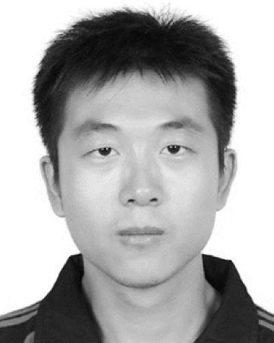 Wang Lingfei (汪令飞)合作论文数Institute of Microelectronics of the Chinese Academy of Sciences30
 Jinshun Bi (毕津顺)合作论文数University of Chinese Academy of Sciences;Institute of Microelectronics of the Chinese Academy of Sciences30
 Writam Banerjee合作论文数Lab. of Nanofabrication & Novel Device Integration, Inst. of Microelectron.;c;Lab. of Nanofabrication & Novel Device Integration, Inst. of Microelectron.30
 Deyu Tu合作论文数30Haitao Sun合作论文数29
 Xiaolong Zhao (赵晓龙)合作论文数School of Integrated Circuits, University of Science and Technology of China;Institute of Advanced Technology, University of Science and Technology of China28
 Weihua Guan合作论文数School of Electrical Engineering and Computer Science, College of Engineering, The Pennsylvania State University28Yingtao Li (李颖弢)合作论文数School of Physical Science and Technology, Lanzhou University, Lanzhou 730000, China28Zhang Sen (张森)合作论文数27
 Hong Wang (王宏)合作论文数School of Microelectronics, Xidian University27
 Junning Chen (陈军宁)合作论文数School of Electronic Science and Technology,Anhui University27
 Guangwei Xu (徐光伟)合作论文数School of Integrated Circuits, University of Science and Technology of China26Xichen Chuai合作论文数25Jiawei Wang合作论文数LIB Engineering Laboratory, Materials Science and Technology Center25
 Xinghua Liu合作论文数25
 Wei Wang合作论文数23Meiyun Zhang (张美芸)合作论文数23
 Su Liu (刘肃)合作论文数School of Physical Science and Technology Lanzhou University23
 Xiaonan Yang (杨潇楠)合作论文数School of Electrical and Information Engineering, Zhengzhou University23
 Yang Li (李阳)合作论文数Xiamen Institute of Rare Earth Materials Haixi Institutes, Chinese Academy of Sciences23




