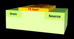
Ferroelectric field effect transistors (FeFETs) are among the most promising candidates for the implementation of artificial synapses for neuromorphic computing. However, their scaling poses big challenges, as multilevel behavior is hindered by the two-level or very-few-level polarization behavior reported for devices featuring an aggressive lateral scaling. Moreover, the switching and stabilization of ferroelectric polarization, and consequently the device operation, is inherently linked to high levels of charge trapping in the gate stack, limiting the reliability and increasing the variability of the FeFETs. In this work we investigate, by means of calibrated TCAD simulations, FeFETs integrating a metal interlayer inside the gate stack. FeFETs are designed so that, by properly biasing the device, the metal interlayer can get charged thanks to charge tunneling through the dielectric layer. We first investigate a conventional front-end-of-line implementation, consisting of an aggressively scaled FeFET featuring a ferroelectric hafnium zirconium oxide and a dielectric hafnium oxide in the gate stack, a single-crystal silicon channel, and highly-doped source and drain pockets. Then we consider a back-end-of-line compatible device structure featuring lightly– doped amorphous gallium-oxide channel material, with Schottky-type tungsten contacts. We show that, for both architectures, the charge in the metal interlayer can effectively stabilize the ferroelectric polarization, even for a negligible charge trapping in the dielectric stack. Moreover, the interplay between ferroelectric polarization and charge in the metal interlayer enables a multilevel operation even for a uniform ferroelectric polarization.
Ferroelectric Tunnel Junctions (FTJs) performance as memristive devices is typically represented by their Tunneling Electro-Resistance Ratio (TER), defined as the ratio between the DC current measured in the low resistance state (LRS) and in the high-resistance state (HRS) of the device. However, during characterization of the FTJ read current and hence of TER, the transient contributions to the current are often overlooked in the literature, possibly causing misleading interpretations of the experimental TER. Here we propose a new, comprehensive characterization of the readout currents of different FTJ stacks, also investigating on their transient components. We report a solid interpretation of the experiments based on the response of traps in the ferroelectric, also supported by physics-based simulations.
We present an ab-inito transport study, based on the Density Functional Theory (DFT) and the non-equilibrium Green's Functions (NEGF) formalism, to assess the effect of the Image Force Barrier Lowering (IFBL) on the source-tochannel resistance ($R_{\mathbf{C}}$) in metal-MoS2 top contacts. To compute the IFBL potential profile, our model relies on the numerical solution of the 3D Poisson equation for the point charge in a heterogeneous dielectric environment. By considering Al-MoS2 and Bi-MoS2 van-der-Waals heterojunctions, representative of a Schottky and an Ohmic contact respectively, we show that, while for Schottky contacts the inclusion of the IFBL has a vast impact on the source-to-channel resistance, in quasi-Ohmic contacts the influence of the IFBL on the $R_{\mathbf{C}}$ becomes negligible, especially at large inversion densities.
Multi-level operation, conventionally obtained in ferroelectric devices thanks to a domain-dependent inhomogeneous polarization, poses a big challenge for highly-scaled ferroelectric devices, where the number of ferroelectric domains is drastically reduced. In this work, we study a highly scaled back-end-of-line (BEOL) compatible, ferroelectric field-effect transistor (FeFET) that integrates a metal interlayer in the gate stack. Through analytical models and calibrated TCAD simulations, we show how this device can achieve a multi-level operation exploiting the interplay between the ferroelectric polarization and the charge in the metal interlayer. Such a working principle does not rely on a domain-dependent inhomogeneous polarization, and the device operation is thus ensured also for a homogeneous ferroelectric material. We also demonstrate that the charge in the interlayer can effectively stabilize the ferroelectric polarization even in the absence of a high concentration of trapped charges in the gate stack. The potentiation and depression curves for the readout conductance confirm that the proposed device can be operated as a memristor for neuromorphic computing applications. Moreover, we show how the choice of the dielectric in the metal-ferroelectric-dielectric-metal gate stack can be used as a design knob to reduce the device operation voltage.
We present a critical reexamination of the Landau-Ginzburg-Devonshire (LGD) model for ferroelectric materials that is based on intrinsic nucleation events. Theoretical considerations and a systematic comparison with experiments steered us towards a novel version and calibration of the LGD model relying instead on extrinsic nucleations. We show that the new model can not only improve the agreement with experiments, but also help reconcile the interpretation of polarization reversal in poly-crystalline and epitaxial ferroelectrics.
The demand for hardware platforms that can enable an efficient execution of artificial intelligence algorithms is on the rise. As the logic-memory separation in the von Neumann architecture is responsible for a large part of the energy consumption and latency, in-memory computing and neuromorphic computing are emerging as promising paradigms to reduce power consumption and delay thanks to the co-localization of processing and memory functionalities. It has been shown that Schottkyjunction devices can be used to realize versatile transistors, able to be reconfigured at run-time between n- and p-type behavior, without the need of doping. The addition of a ferroelectric gate can be exploited to tune the Schottky barrier in a non-volatile manner, effectively realizing logic devices whose behavior can be influenced by the ferroelectric remnant polarization, merging logic and memory functionalities. In this work we present an optimized fabrication scheme that allows for the fabrication of ferroelectrically-tuned Schottky-junction devices with improved TiN gate structures. Furthermore, to better understand the device behavior, we present TCAD simulations calibrated on fabricated structures.
We present a fabricated and experimentally characterized memory stack that unifies memristive and memcapacitive behavior. Exploiting this dual functionality, we design a circuit enabling simultaneous control of spatial and temporal dynamics in recurrent spiking neural networks (RSNNs). Hardware-aware simulations highlight its promise for efficient neuromorphic processing.
This work presents a simulation study of a ferroelectric field effect transistor (FeFET), which leverages a metal interlayer to achieve a multilevel operation thanks to the interplay between the ferroelectric polarization and the charge stored in the interlayer. We show that the metal interlayer can effectively stabilize the ferroelectric polarization even for a negligible charge trapping in the dielectric stack and, moreover, enable a multilevel operation even for a uniform ferroelectric polarization.
The development of data-centric computing requires new energy-efficient electronics that can overcome the fundamental limitations of conventional silicon transistors. A range of novel transistor concepts have been explored, but an approach that can simultaneously offer high drive current and steep slope switching while delivering the necessary scaling in footprint is still lacking. Here, we report scaled vertical-nanowire heterojunction tunnelling transistors that are based on the broken-band GaSb/InAs system. The devices offer a drive current of 300 mu A mu m-1 and a sub-60 mV dec-1 switching slope at an operating voltage of 0.3 V. The approach relies on extreme quantum confinement at the tunnelling junction and is based on an interface-pinned energy band alignment at the tunnelling heterojunction under strong quantization. Vertical-nanowire heterojunction tunnelling transistors that are based on the broken-band GaSb/InAs system can offer a drive current of 300 mu A mu m-1 and a sub-60 mV dec-1 switching slope at an operating voltage of 0.3 V.
We present analytical models and numerical simulations addressing the fundamental limits to the sub-threshold swing (SS) in Dirac-Source FETs (DS-FETs), based on either graphene or 3D Dirac semimetals. To this purpose, we devised and implemented a semi-analytical model for DS-FETs employing a 3D Dirac source. Numerical results confirm analytical predictions. Our findings help to clarify the physics behind the minimum SS in DS-FETs, and the possible advantages offered by 3D Dirac semimetals.
In this paper we first present a model based on the transfer-matrix methodology to describe the ballistic resistance in a graphene p - n junction, and employ the model in Dirac-Source FETs. In fact, the access region of a graphene based Dirac-Source FET includes a p - n junction, and we show that this has a sizeable impact on the on-state current of these transistors. In particular, we first validate our model by comparing the calculated p - n junction resistance with previous experiments and simulations. Then, we exploit the transfer-matrix description into a virtual-source model for nanoscale Dirac-Source FETs, and discuss the influence on the I-DS - V(GS )curves of the p - n junction that is embedded in the access region of the device.
We investigate the application of the Eligibility Propagation (E-prop) learning algorithm to train an adiabatic neuromorphic circuit that emulates Leaky Integrate-and-Fire (LIF) neuron dynamics with ultra-low power consumption. Using a tactile Braille digit classification task as a benchmark, we adapted the model to the constraints of the adiabatic hardware. Our 450-neuron, Recurrent Spiking Neural Network (RSNN) achieved a peak test accuracy of 91.1 % after 25 training epochs, with an average best accuracy of 88.72 % (+/- 1.63 %) across multiple runs. While E-prop enabled efficient local learning under hardware limitations, it underperformed compared to Backpropagation Through Time (BPTT), which achieved 98 % accuracy. These results highlight the promise of E-prop for learning in spike-based systems and point to the need for further optimization to close the performance gap.
Switching dynamics of ferroelectric (FE) based devices not only depend on the FE material but also on the design options available for the materials stack. However, the impact of the design of the material layers on the FE device properties is not fully understood yet. Here, we report a comprehensive characterization of Ferroelectric Tunnel Junctions based on Metal-Ferroelectric-Dielectric-Metal (MFDM) stacks and a full benchmark of the extracted parameters with those of Metal-Ferroelectric-Metal (MFM) capacitors. MFDM devices show an evident dependence of the extracted coercive voltages on the thickness of the dielectric layer (DE), as well as on the frequency of the signal used to characterize the device, which is not observed in MFM stacks. Finally, the remnant polarization measured in MFDM stacks is lower than in MFM samples. Together, all these evidences suggest that the traps at the FE-DE interface play a fundamental role in the switching dynamics of the device and in the extraction of the ferroelectric parameters.
The progress of biologically inspired neuromorphic computing hardware in the last decade has been fostered also by the advancement in CMOS-compatible memristors, providing a nonvolatile storage of multiconductance states mimicking the synaptic weights in biological systems. This article is instead focused on the less-explored field of memcapacitors (MemCaps), which only very recently has attracted a renewed interest, and it is based on devices capable of tuning their capacitance. In particular, we present by means of extensive numerical simulations carefully calibrated against experimental data the operation of a two-terminal ferroelectric MemCap exhibiting multilevel, polarization-dependent capacitance values. The MemCap exploits a ferroelectric gated-diode structure, and it is thus fully compatible with CMOS processing. Our results show that multilevel operation is viable using properly shaped pulse trains at the gate terminal, and moreover, a nondestructive readout can be achieved by means of small-amplitude ac signals.
This paper studies the impact of the access region on the on-state current of Dirac-Source FETs. To this purpose, we develop a transfer-matrix model for graphene p-n junctions and FETs, and validate it with experiments. Our analysis provides insights about the operation and design of these novel computing devices.
In recent years, the In-Memory-Computing in charge domain has gained significant interest as a promising solution to further enhance the energy efficiency of neuromorphic hardware. In this work, we explore the synergy between the brain-inspired computation and the adiabatic paradigm by presenting an adiabatic Leaky Integrate-and-Fire neuron in 180 nm CMOS technology, that is able to emulate the most important primitives for a valuable neuromorphic computation, such as the accumulation of the incoming input spikes, an exponential leakage of the membrane potential and a tunable refractory period. Differently from previous contributions in the literature, our design can exploit both the charging and recovery phases of the adiabatic operation to ensure a seamless and continuous computation, all the while exchanging energy with the power supply with an efficiency higher than 90% over a wide range of resonance frequencies, and even surpassing 99% for the lowest frequencies. Our simulations unveil a minimum energy per synaptic operation of 360 fJ at a 500 kHz resonance frequency, which yields a 12x energy saving with respect to a non-adiabatic operation.
The energy efficiency of ferroelectric-based devices makes them interesting for many applications. However, their optimization requires a dependable characterization of the ferroelectric (FE) material. In this work, we show and investigate how the series resistance (R S ) can strongly impact the current-voltage (I-V) characteristics of Metal-Ferroelectric-Metal (MFM) stacks and distorts the hysteresis curves, which can lead to an inaccurate extraction of the FE parameters and a misleading interpretation of FE switching dynamics. The complex R S effect on the I-V curves cannot be easily compensated, so here we propose, for the first time to our knowledge, a procedure for an improved extraction of the FE parameters even in the presence of a non-negligible series resistance.
By using a modelling framework consisting of NEGF-based ab-initio simulations, we investigate the operation and design of Dirac-Source FETs (DSFETs). First, we discuss some methodological aspects that we found pivotal to observe the sub-60mV/dec swing in ab-initio simulations. Then, we propose the novel HGr-DSFET based on hydro-genated graphene (HGr). We show that the HGr-DSFET has a robust sub-60mV/dec operation and an ON current between $2\times$ and $4\times$ larger than the graphene-MoS2 DSFET counterpart. Our study addresses and elucidates several physical and design aspects of DSFETs, including the rethermalization effects due to phonon scattering.
A self-consistent Monte Carlo/3-D Poisson simulator has been developed to analyze the current asymmetry in graphene geometric diodes. The model couples ballistic transport in the graphene layer with 3-D electrostatics in the graphene and oxide substrate. Results are given in terms of transmission coefficients and currents at the two terminals of the diode. We prove that while the current asymmetry is mainly induced by ballistic transport in the asymmetric structure, the electrostatics plays a relevant role that tends to substantially counterbalance the geometrical effect.
A primary objective of Spiking Neural Networks is a very energy-efficient computation. To achieve this target, a small spike rate is of course very beneficial given the event-driven nature of such a computation. A network that processes information encoded in spike timing can, by its nature, have such a sparse event rate, but, as the network becomes deeper and larger, the spike rate tends to increase without any improvements in the final accuracy. If, on the other hand, a penalty on the excess of spikes is used during the training, the network may shift to a configuration where many neurons are silent, thus affecting the effectiveness of the training itself. In this paper, we present a learning strategy to keep the final spike rate under control by changing the loss function to penalize the spikes generated by neurons after the first ones. Moreover, we also propose a 2-phase training strategy to avoid silent neurons during the training, intended for benchmarks where such an issue can cause the switch off of the network.
 Luca Selmi合作论文数Dipartimento di Ingegneria Enzo Ferrari, Università degli Studi di Modena e Reggio Emilia;University of Udine187
 Pierpaolo Palestri合作论文数Dipartimento Politecnico di Ingegneria e Architettura, University of Udine167
 Francesco Driussi合作论文数DIEGM, University of Udine – IU.NET71
 Daniel Lizzit合作论文数38
 Marco G. Pala合作论文数Dipartimento di Ingegneria;dell ' Informazione;Universita degli Studi di Pisa;Dipartimento di Ingegneria|dell ' Informazione, Universita degli Studi di Pisa27
 Enrico Sangiorgi合作论文数University of Bologna26
 Claudio Fiegna合作论文数26
 Enrico Caruso合作论文数DIEGM, Univ. of Udine;c;DIEGM, Univ. of Udine21
 F. Conzatti合作论文数DIEGM and IU.NET, University of Udine16
 Marco Massarotto合作论文数15Mattia Segatto合作论文数DPIA, Univ Udine14
 Tommaso Rollo合作论文数14
 Bruno Riccó合作论文数University of Bologna14
 M. De Michielis合作论文数DIEGM, University of Udine14
 Sebastiano Strangio合作论文数13
 Felice Crupi合作论文数a;Dipartimento di Fisica della Materia e Tecnologie Fisiche Avanzate and INFM;a; Dipartimento di Fisica della Materia e Tecnologie Fisiche Avanzate and INFM13
 Riccardo Fontanini合作论文数DPIA, Univ Udine12
 Alan Paussa合作论文数Dipt. di Ing. Elettr., Gestionale e Meccanica, Univ. of Udine;c12
 A. Pilotto合作论文数DPIA, University of Udine11
 van Duuren, M.合作论文数11Luca Lucci合作论文数11
 Ruben Specogna合作论文数Polytech Dept Engn & Architecture, Univ Udine11
 Massimo Bruno Alioto合作论文数Department of Electrical and Computer Engineering, College of Design and Engineering, National University of Singapore11
 Stefan Slesazeck合作论文数NaMLab gGmbH, Dresden, Germany10
 Marco Lanuzza合作论文数University of Calabria10
 Patrik Osgnach合作论文数10p toniutti合作论文数9
 Pedram Khakbaz合作论文数Polytech Dept Engn & Architecture, Univ Udine9
 Thomas Mikolajick合作论文数Center for Advancing Electronics Dresden, Dresden University of Technology9
 Mirko Loghi合作论文数9S. Eminente合作论文数8
 Suzanne Lancaster合作论文数NaMLab gGmbH, D-01187 Dresden, Germany8
 Antonio Arreghini合作论文数8
 Elisa Vianello合作论文数CEA-Leti8
 Antonio Abramo合作论文数8O. Badami合作论文数7
 Frans.P. Widdershoven合作论文数Department of Microelectronics, Faculty of Electrical Engineering, Mathematics and Computer Science, Delft University of Technology7
 Elena Gnani合作论文数Department of Electrical, Electronic, and Information Engineering "Guglielmo Marconi", Alma Mater Studiorum - Università di Bologna;"Ercole De Castro" Research Centre on Electronic Systems for Information and Communication Technologies, Alma Mater Studiorum - Università di Bologna7
 N. Akil合作论文数Philips Research Leuven7
 Andreas Schenk (至遠空)合作论文数Department of Information Technology and Electrical Engineering, Eidgenossische Technische Hochschule Zurich7
 Mikael Östling合作论文数Division of Electronics and Embedded Systems, KTH Royal Insititute of Technology;Faculty of EE, KTH Royal Institute of Technology6
 Stefano Venica合作论文数6
 Paolo Giannozzi合作论文数Department of Mathematics, Computer Science, and Physics, University of Udine6
 Karim Cherkaoui合作论文数Tyndall National Institute, University College Cork6
 Alessandro Cresti合作论文数IMEP-LAHC (UMR CNRS/INPG/UJF 5130), Grenoble INP Minatec6
 David R. Leadley合作论文数Department of Physics;University of Warwick;Department of Physics, University of Warwick6
 George K. Celler合作论文数University of Wisconsin-Madison6
 Farzan Gity合作论文数Tyndall National Institute, University College Cork6
 Scott Monaghan合作论文数Tyndall National Institute, University College Cork6




