This paper presents a dynamic frequency scaling (DFS) technique, PIDDFS, targeting on real-time applications running on GPU platforms. PIDDFS technique applies a feedback controlling algorithm, Proportional-Integral-Derivative (PID), to scale the frequencies of core domain and DRAM domains based on memory access statistics. The major goal of PIDDFS is minimizing the energy consumption while the memory traffic is intensive or even causes the pipeline to stall. Performance can also be improved via increasing the frequency while the memory traffic is in a starving status. Based on the feedback, closed-loop controlling model with proper leading and lagging phases, PIDDFS can respond timely towards the variations during runtime and ignore the insignificant noise that causes unnecessary frequency adjustments. The proposed technique has been simulated on GPGPU-Sim, a cycle-level simulator of GPU architecture and power savings have been modeled by GPUWattch. According to the benchmark simulation result, a power saving of more than 23% with a performance improvement of 4% is achieved at the same time. Stalled cycles caused by saturation of memory request queues are reduced over 40%.
Quantum mechanical principles that govern the basic laws of physics increasingly limit CMOS operation with transistor scaling. Traditional logic based CMOS circuits cannot achieve ultra-low power levels due to heat dissipated for a single bit loss of information as represented by the Landauer barrier. Reversible logic is a promising computing paradigm towards realization of ultra-low power computing circuits. Reducing average and peak power consumption is an effective strategy for mitigation of side-channel attacks, such as Differential Power Analysis. We present designs of Forward Body Biased Adiabatic Logic for reduction of average, peak, and differential power. HSPICE simulations with predictive 22nm technology are used to analyze performance metrics and exhaustive simulation results are presented for various reversible CMOS designs. Average power is improved upon by up to 91%, the peak power by up to 96%, and the differential power is improved by up to a factor of 128.57.
Reversible logic is a computing paradigm in which there is a one to one mapping between the input and the output vectors. Reversible logic gates are implemented in an optical domain as it provides high speed and low energy computations. In the existing literature there are two types of optical mapping of reversible logic gates: (i) based on a semiconductor optical amplifier (SOA) using a Mach–Zehnder interferometer (MZI) switch; (ii) based on linear optical quantum computation (LOQC) using linear optical quantum logic gates. In reversible computing, the NAND logic based reversible gates and design methodologies based on them are widely popular. The NOR logic based reversible gates and design methodologies based on them are still unexplored. In this work, we propose two NOR logic based n-input and n-output reversible gates one of which can be efficiently mapped in optical computing using the Mach–Zehnder interferometer (MZI) while the other one can be mapped efficiently in optical computing using the linear optical quantum gates. The proposed reversible NOR gates work as a corresponding NOR counterpart of NAND logic based Toffoli gates. The proposed optical reversible NOR logic gates can implement the reversible boolean logic functions with a reduced number of linear optical quantum logic gates or reduced optical cost and propagation delay compared to their implementation using existing optical reversible NAND gates. It is illustrated that an optical reversible gate library having both optical Toffoli gate and the proposed optical reversible NOR gate is superior compared to the library containing only the optical Toffoli gate: (i) in terms of number of linear optical quantum gates when implemented using linear optical quantum computing (LOQC), (ii) in terms of optical cost and delay when implemented using the Mach–Zehnder interferometer.
Reversible computing is based on logic circuits that can generate unique output vector from each input vector, and vice versa, that is, there is a one-to-one mapping between the input and the output vectors. Reversible computing is the only solution for non-dissipative ultra low power green computing. Conservative reversible circuits are a specific type of reversible circuits, in which there would be an equal number of 1s in the outputs as there would be on the inputs, in addition to one-to-one mapping. This work illustrates the application of reversible logic towards testing of faults in traditional and reversible field coupled nanocircuits (Portions of this chapter are based on [2]. The enhancement is comprehensive treatment of: basics of reversible computing, motivation for reversible computing, background on conservative logic, basics of QCA computing, such as QCA logic devices and QCA clocking, related work etc. Several new reversible testable designs are introduced such as design of testable reversible T latch, design of testable asynchronous set/reset D latch and master-slave D flip-flop, design of testable reversible complex sequential circuits. QCA layouts of conservative logic gates are introduced with internal design details of QCA logic devices. Complete fault patterns information and analysis are provided for conservative logic gates. The synthesis of non-reversible testable design based on MX-cqca gate is extended to MX-cqca based implementation of standard functions. The significance of this work and broader prospective for future directions is also presented.). We propose the design of two vectors testable sequential circuits based on conservative logic gates. The proposed sequential circuits based on conservative logic gates outperform the sequential circuits implemented in classical gates in terms of testability. Any sequential circuit based on conservative logic gates can be tested for classical unidirectional stuck-at faults using only two test vectors. The two test vectors are all 1s, and all 0s. The designs of two vector testable latches, master-slave flip-flops, double edge triggered flip-flops, asynchronous set/reset D latch and D flip-flop are presented. The importance of the proposed work lies in the fact that it provides the design of reversible sequential circuits completely testable for any stuck-at fault by only two test vectors, thereby eliminating the need for any type of scan-path access to internal memory cells. The reversible designs of the double edge triggered flip-flop, ring counter and Johnson Counter are proposed for the first time in literature. We are showing the application of the proposed approach towards 100 % fault coverage for single missing/additional cell defect in the QCA layout of the Fredkin gate. We are also presenting a new conservative logic gate called Multiplexer Conservative QCA gate (MX-cqca) that is not reversible in nature but has similar properties as the Fredkin gate of working as 2:1 multiplexer. The proposed MX-cqca gate surpasses the Fredkin gate in terms of complexity (the number of majority voter), speed and area.
In this paper, we propose the design of two vectors testable sequential circuits based on conservative logic gates. The proposed sequential circuits based on conservative logic gates outperform the sequential circuits implemented in classical gates in terms of testability. Any sequential circuit based on conservative logic gates can be tested for classical unidirectional stuck-at faults using only two test vectors. The two test vectors are all 1's, and all 0's. The designs of two vectors testable latches, master-slave flip-flops and double edge triggered (DET) flip-flops are presented. The importance of the proposed work lies in the fact that it provides the design of reversible sequential circuits completely testable for any stuck-at fault by only two test vectors, thereby eliminating the need for any type of scan-path access to internal memory cells. The reversible design of the DET flip-flop is proposed for the first time in the literature. We also showed the application of the proposed approach toward 100% fault coverage for single missing/additional cell defect in the quantum-dot cellular automata (QCA) layout of the Fredkin gate. We are also presenting a new conservative logic gate called multiplexer conservative QCA gate (MX-cqca) that is not reversible in nature but has similar properties as the Fredkin gate of working as 2:1 multiplexer. The proposed MX-cqca gate surpasses the Fredkin gate in terms of complexity (the number of majority voters), speed, and area.
Reversible logic is gaining significance in the context of emerging technologies such as quantum computing since reversible circuits do not lose information during computation and there is one-to-one mapping between the inputs and outputs. In this work, we present a class of new designs for reversible binary and BCD adder circuits. The proposed designs are primarily optimized for the number of ancilla inputs and the number of garbage outputs and are designed for possible best values for the quantum cost and delay. In reversible circuits, in addition to the primary inputs, some constant input bits are used to realize different logic functions which are referred to as ancilla inputs and are overheads that need to be reduced. Further, the garbage outputs which do not contribute to any useful computations but are needed to maintain reversibility are also overheads that need to be reduced in reversible designs. First, we propose two new designs for the reversible ripple carry adder: (i) one with no input carry c0 and no ancilla input bits, and (ii) one with input carry c0 and no ancilla input bits. The proposed reversible ripple carry adder designs with no ancilla input bits have less quantum cost and logic depth (delay) compared to their existing counterparts in the literature. In these designs, the quantum cost and delay are reduced by deriving designs based on the reversible Peres gate and the TR gate. Next, four new designs for the reversible BCD adder are presented based on the following two approaches: (i) the addition is performed in binary mode and correction is applied to convert to BCD when required through detection and correction, and (ii) the addition is performed in binary mode and the result is always converted using a binary to BCD converter. The proposed reversible binary and BCD adders can be applied in a wide variety of digital signal processing applications and constitute important design components of reversible computing.
Conservative reversible logic gate is a reversible logic gate that is reversible in nature and also satisfy the property that there are equal number of 1s in the outputs as in the inputs. In this work, we present a new class of n × n (n inputs and n outputs) conservative reversible logic gate named SCRL (Super Conservative Reversible Logic) gate for the design of reversible quantum circuits. The proposed SCRL gate has 1 control input depending on the value of which it can swap any two n - 1 data inputs, hence is superior to the existing Fredkin gate. In reversible circuits, the constant input bits that are used to realize different logic functions are referred to as ancilla inputs, while the outputs that are neither primary inputs nor contribute to any useful computations are referred to as garbage outputs. As Ancilla inputs and garbage outputs are overhead bits in a reversible circuit, they need to be minimized. Barrel shifter forms an integral component of many computing systems. As an example of using the proposed SCRL gate to design efficient reversible quantum circuits, the design of reversible barrel shifter with zero ancilla inputs and zero garbage outputs is illustrated.
Reversible logic is emerging as a promising computing paradigm with applications in ultralow power nanocomputing and emerging nanotechnologies such as quantum computing, quantum dot cellular automata (QCA), optical computing, etc. Reversible circuits are similar to conventional logic circuits except that they are built from reversible gates. In reversible gates, there is a unique, one-to-one mapping between the inputs and outputs, not the case with conventional logic. One of the primary motivations for adopting reversible logic lies in the fact that it can provide a logic design methodology for designing ultra-low power circuits beyond KTln2 limit for those emerging nanotechnologies in which the energy dissipated due to information destruction will be a significant factor of the overall heat dissipation. Further, logic circuits for quantum computers must be built from reversible logic components. Several important metrics need to be considered in the design of reversible circuits the importance of which needs to be discussed. Quantum computers of many qubits are extremely difficult to realize thus the number of qubits in the quantum circuits needs to be minimized. This sets the major objective of optimizing the number of ancilla inputs and the number of the garbage outputs in the reversible logic based quantum circuits. The constant input in the reversible quantum circuit is called the ancilla input, while the garbage output refers to the output which exists in the circuit just to maintain one-to-one mapping but is not a primary or a useful output. The reversible circuit has other important parameters of quantum cost and delay which need to be optimized.
Reversible logic has promising applications in dissipation less optical computing, low power computing, quantum computing etc. Reversible circuits do not lose information, and there is a one to one mapping between the input and the output vectors. In recent years researchers have implemented reversible logic gates in optical domain as it provides high speed and low energy computations. The reversible gates can be easily fabricated at the chip level using optical computing. The all optical implementation of reversible logic gates are based on semiconductor optical amplifier (SOA) based Mach-Zehnder interferometer (MZI). The Mach-Zehnder interferometer has advantages such as high speed, low power, easy fabrication and fast switching time. In the existing literature, the NAND logic based implementation is the only implementation available for reversible gates and functions. There is a lack of research in the direction of NOR logic based implementation of reversible gates and functions. In this work, we propose the NOR logic based all optical reversible gates referred as all optical TNOR gate and all optical PNOR gate. The proposed all optical reversible NOR logic gates can implement the reversible boolean logic functions with reduced optical cost and propagation delay compared to their implementation using existing all optical reversible NAND gates. The advantages in terms of optical cost and delay is illustrated by implementing 13 standard boolean functions that can represent all 256 possible combinations of three variable boolean function.
In this work, we investigate state-retentive power gating of register files for leakage reduction in multicore processors supporting multithreading. In an in-order core, when a thread gets blocked due to a memory stall, the corresponding register file can be placed in a low leakage state through power gating for leakage reduction. When the memory stall gets resolved, the register file is activated for being accessed again. Since the contents of the register file are not lost and restored on wakeup, this is referred to as state-retentive power gating of register files. While state-retentive power gating in single cores has been studied in the literature, it is being investigated for multicore architectures for the first time in this work. We propose specific techniques to implement state-retentive power gating for three different multicore processor configurations based on the multithreading model: 1) coarse-grained multithreading, 2) fine-grained multithreading, and 3) simultaneous multithreading. The proposed techniques can be implemented as design extensions within the control units of the in-order cores. Each technique uses two different modes of leakage states: low-leakage savings and low wake-up and high-leakage savings and high wake-up latency. The overhead due to wake-up latency is completely avoided in two techniques while it is hidden for most part in the third approach, either by overlapping the wake-up process with the thread context switching latency or by executing instructions from other threads ready for execution. The proposed techniques were evaluated through simulations with multiprogrammed workloads comprised of SPEC 2000 integer benchmarks. Experimental results show that in an 8-core processor executing 64 threads, the average leakage savings were 42 percent in coarse-grained multithreading, while they were between seven percent and eight percent for finegrained and simultaneous multithreading.
Reversible logic has promising applications in the field of quantum computing, optical computing, low power computing, and other emerging computing technologies. A barrel shifter that can shift and rotate multiple bits in a single cycle is an important component of many computing units. This paper presents the reversible design of bidirectional arithmetic and logical barrel shifter. The proposed design consists of the reversible Fredkin and Feynman gates. The Fredkin gate used in the design of reversible bidirectional arithmetic and logical barrel shifter can implement the 2:1 MUX with minimum quantum cost, minimum number of ancilla bits and minimum number of garbage outputs while the Feynman gate is used to avoid the fanout as fanout is not allowed in the reversible logic. The design is evaluated in terms of number of garbage outputs, quantum cost and number of ancilla bits.
Bosch process is widely used in the fabrication of through silicon via (TSV) holes for 3-D integrated circuit and 3-D Packaging applications mainly due to its high silicon etch rate and selectivity to mask. However, the adverse impact on the electrical performance of the TSV due to the sidewall scallops or wavy profile due to the cyclical nature of the Bosch process has not been thoroughly investigated. This paper therefore focuses on the impact of sidewall scallops on the inter-via electrical leakage performance. Based on finite element analysis, this paper describes that the high stress concentration on the dielectric and barrier layers at the sharp scallops can potentially contribute to barrier failure. It is demonstrated that by smoothening the sidewalls of the TSV, the thermo-mechanical stresses on the dielectric and tantalum barrier is significantly reduced. A test vehicle is designed and fabricated with different geometry of deep silicon vias to study the impact of sidewall profile smoothening for different copper diffusion barrier stacks. It is experimentally demonstrated that the inter-via electrical leakage current can be reduced by almost three orders of magnitude when the sidewall roughness is reduced or replaced by a smoother sidewall. It is also indicated that it is sufficient to smoothen the initial few micrometers of the TSV depth by using a non-Bosch etch process. It is concluded that the Bosch etch process can still be used, with all its merits of high etch rate and high etch selectivity, by tailoring a short initial etch step to smoothen the top sidewalls to minimize the adverse effects of the sidewall scallops.
A novel two step etch process using the Bosch-etch mechanism to prevent notching on an SOI wafer is presented. The first etch step is used to attain the maximum etch depth with high etch rate and stop before the buried oxide (BOX). Followed by the second etch step with lower etch rate and tuned to soft land on the BOX to etch the remaining depth. In addition to that it is tailored to also provide a tapered etch profile which is beneficial in reducing the notch if over etching occurs.
The continuous push for smaller bump pitch interconnection in line with smaller Cu/low-k technology nodes demands the substrate technology to support finer interconnection. However, the conventional organic buildup substrate is facing a bottleneck in fine-pitch wiring due to its technology limitation, and the cost of fabricating finer pitch organic substrate is higher. To address these needs, Si interposer with through silicon via (TSV) has emerged as a good solution to provide high wiring density interconnection, and at the same time to minimize coefficient of thermal expansion mismatch to the Cu/low-k chip that is vulnerable to thermal-mechanical stress and improve electrical performance due to shorter interconnection from the chip to the substrate. This paper presents the development of TSV interposer technology for a 21 × 21 mm Cu/low-k test chip on flip chip ball grid array (FCBGA) package. The Cu/low-k chip is a 65-nm nine-metal layer chip with 150-μm SnAg bump pitch of total 11 000 I/O, with via chain and daisy chain for interconnect integrity monitoring and reliability testing. The TSV interposer size is 25 × 25 × 0.3 mm with CuNiAu as under bump metallization on the top side and SnAgCu bumps on the underside. The conventional bismaleimide triazine substrate size is 45 × 45 mm with BGA pad pitch of 1 mm and core thickness of 0.8 mm. Mechanical and thermal modeling and simulation for the FCBGA package with TSV interposer have been performed. TSV interposer fabrication processes and assembly process of the large die mounted on TSV interposer with Pb-free solder bumps and underfill have been set up. The FCBGA samples have passed moisture sensitivity test and thermal cycling reliability testing without failures in underfill delamination and daisy chain resistance measurements.
The building blocks of the 3-D IC integration technology are Through-Silicon Via (TSV) fabrication/implementation, thin wafer handling, low-temperature backside TSV revealing process, and electrical redistribution or connection of vertical circuitry or ICs. Of these elements, the scheme for wafer thinning and backside passivation is a crucial technology element of 3D integration. In this paper, novel backside via revealing and passivation for 3D IC application is proposed with newly developed process integration. Si/Cu CMP process is applied to overcome the practical limitations on the uniformity of the backside thinning originated from the blind thinning process. As such, the height variations associated with via etch non-uniformity and glue, carrier and grinding TTV's (Total Thickness Variation) are flattened out. In order to protrude the TSV from the backside, we demonstrated new spin wet etchback process with well-controlled repeatability, reduced process defect and copper contamination. For the low-k thick dielectric layer application (without photo-litho), Insulation layer on the back side is deposited over the protruded portion of the TSV structure. The deposited insulation layer is removed and TSV area is again exposed. The process for removing this insulation layer is the plasma etching or CMP polish.
This note describes a new high-throughput process of polyimide etching for the fabrication of MEMS devices with an organic sacrificial layer approach. Using dual frequency superimposed capacitively coupled plasma we achieved a vertical profile of polyimide with an etching rate as high as 3.5 µm min−1. After the fabrication of vertical structures in a polyimide material, additional steps were performed to fabricate structural elements of MEMS by deposition of a SiO2 layer and performing release etching of polyimide.
Nowadays, GPU architecture is commonly exploited in various researches on computer graphic and other scientific computing areas. Parallel computing feature of GPU provides performance benefits for execution of many programs. However, as the parallel degree keeps extending, the number of active cores in GPU required for execution is also increasing. Therefore the rising of energy consumption caused by using large number of cores begins to draw attention. Previous research [1] reveals that given a multicore program, the curve of energy consumption first falls and then rises, as the number of active cores increases. That means we can have the minimum energy consumption if the number of active cores is properly configured. In this paper, we develop an instruction-level prediction mechanism to estimate the energy consumption of a given program under different numbers of cores. The prediction is based on the profile of Parallel Thread Execution (PTX) [2] codes generated during compilation of the original program. With the help of this mechanism, the energy-optimal number of cores can be found during compilation and used in execution, replacing the one given by programmer. Tests have been carried on several NVIDIA CUDA [10] benchmarks. The results show that the energy consumption is minimized without losing much performance. With the predicted energy-optimal number of active cores, we show that the energy consumption saving for the selected benchmarks is from 7.31% to 11.76% on average, with a worst case of performance lost 4.92%.
 Himanshu Thapliyal合作论文数Min H. Kao Department of Electrical Engineering and Computer Science, Tickle College of Engineering, University of Tennessee16
 Ramamurti Chandramouli合作论文数Department of Electrical and Computer Engineering
Stevens Institute of Technology14
Ramamurti Chandramouli合作论文数Department of Electrical and Computer Engineering
Stevens Institute of Technology14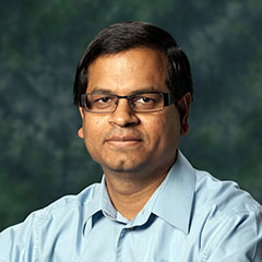 Saraju Mohanty合作论文数Department of Computer Science and Engineering, College of Engineering, University of North Texas13
 Vijaykrishnan Narayanan合作论文数School of Electrical Engineering and Computer Science, College of Engineering, Pennsylvania State University12
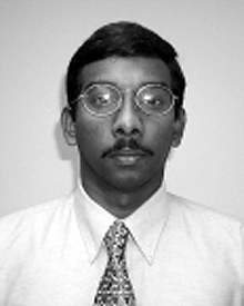 Ashok K. Murugavel合作论文数12
 Sanjukta Bhanja合作论文数Electrical Engineering Department10
 C. S. Premachandran合作论文数Institute of Microelectronics8
 Koustav Bhattacharya合作论文数Department of Computer Science and Engineering, University of South Florida8
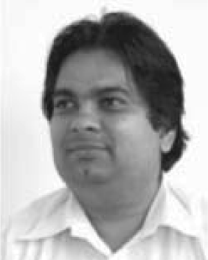 V. Kripesh合作论文数8
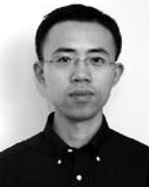 liao ebin合作论文数7Mario Kovac合作论文数7
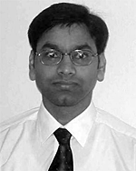 Narender Hanchate合作论文数7
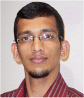 Venkataraman Mahalingam合作论文数6Veeru N. Ramaswamy合作论文数6
 Saurabh Kotiyal合作论文数University of South Florida6
 Narayanana Balasubramanian合作论文数6V Krishna合作论文数5Hitoshi Oi合作论文数5Rajiv Mehrotra合作论文数5Wee-Liat Ong合作论文数Institute of Microelectronics5Raghu Sastry合作论文数5Damaruganath Pinjala合作论文数5
 Levent Yobas合作论文数Department of Electronic & Computer Engineering , The Hong Kong University of Science and Technology5Sunil K. Chappidi合作论文数5Henriques, S.合作论文数4Mi Patel合作论文数4Ravi K. Namballa合作论文数4
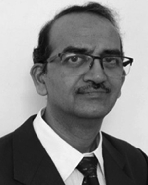 Ajay Agarwal合作论文数4K. Prasad合作论文数4Matthew Morrison合作论文数Medtronic Sofemor Danek4N. Bhavanishankar合作论文数4
 Kin Leong Pey合作论文数4
 Abdel Ejnioui合作论文数Department of Information Technology, University of South Florida4Kum Cheong Tang合作论文数3
 Senthil Kumar合作论文数3michael nachtigal合作论文数3Kameswara Rao Namuduri合作论文数3Nichani, S.合作论文数3
 Rajarathnam Chandramouli合作论文数Department of Electrical and Computer Engineering, School of Engineering and Science, Stevens Institute of Technology3
 Amar Mukherjee合作论文数3
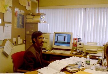 Ravi Sankar合作论文数University of South Florida College of Engineering3Girish Chiruvolu合作论文数3
 Xiaowu Zhang合作论文数Institute of Microelectronics, Agency for Science Technology and Research3
 Upavan Gupta合作论文数University of South Florida3S. J. Ramadoss合作论文数3
 Seung Wook Yoon合作论文数stats chippac ltd3
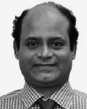 B. Ramana Murthy合作论文数Institute of Microelectronics, A*STAR (Agency for Science, Technology and Research),3Janak Singh合作论文数2R MEHROTRA合作论文数2




