This paper proposes a decision-error correction scheme that improves the pre-forward error correction (pre-FEC) bit-error rate (BER) by identifying and correcting symbol errors after the decision feedback equalizer (DFE) without introducing any coding overhead. The proposed method reconstructs the received waveform to localize error-prone symbols without requiring additional redundancy and performs symbol-level correction by exploiting intrinsic properties of pulse-amplitude modulation (PAM) signaling. The error detection and correction scheme is implemented using simple digital arithmetic and logic and completes the correction process within three digital signal processor (DSP) clock cycles, thereby avoiding excessive latency. A 4-level pulse-amplitude modulation (PAM-4) DSP employing a 64-way parallel datapath was implemented in a 14-nm FinFET process, occupying 0.269 mm2 and targeting an 875 MHz clock frequency. The design was validated on a Xilinx ZCU111 RFSoC platform, demonstrating a BER improvement of more than five orders of magnitude at 4.8 Gb/s over a channel with 22.9 dB insertion loss (IL) at Nyquist.
This article presents a 76-Gb/s digital-to-analog converter (DAC)-based discrete multitone (DMT) wireline transmitter (TX) fabricated in 5-nm FinFET. The TX employs a 16-way parallel multi-path delay feedback (MDF) inverse fast Fourier transform (IFFT) processor for area-efficient implementation. The TX digital signal processor (DSP) includes on-chip bit/power-loading and cyclic-prefix (CP) insertion logic and supports 4- to 256-QAM modulation formats across 31 orthogonal subchannels. The time-domain DMT samples generated by the TX DSP are converted into analog waveform using a source-series termination (SST)-based DAC. The prototype is demonstrated over a channel with 9.7-dB insertion loss (IL) at Nyquist, achieving a bit error rate (BER) of 2.1E-4 with a total power consumption of 144 mW from 0.735-V digital and 0.725-V analog supplies, resulting in an energy efficiency of 1.89 pJ/b. The proposed DMT TX improves bandwidth efficiency and signal-to-noise ratio (SNR) over conventional pulse-amplitude modulation (PAM)-based transmitters by employing frequency-domain modulation and equalization. This work is the first demonstration of a DAC-based DMT TX operating at >76 Gb/s fabricated in advanced CMOS technology.
Dramatic cost reductions driven by private sector innovations have led to a rapid increase in the number of satellites in orbit and a corresponding surge in space-generated data. As this trend continues, transmitting large volumes of data to Earth for processing may become increasingly costly and challenging due to potential space-to-Earth link congestion and increased latency. Moreover, traditional ground station networks may face difficulties accommodating growing data flows and workloads because of capacity constraints, complex scheduling logistics, and restricted visibility windows, which can limit scalability. Space Data Centers (SDCs) – software-driven, multi-tenant artificial intelligence-based service platforms capable of processing data in orbit to generate actionable insights for client satellites and ground users – represent a promising approach to address these challenges. This article presents the architecture of a Low Earth Orbit SDC satellite constellation, considering orbital design, inter-satellite links and network topology, computational resource organization, and software service orchestration. We analyze the potential technical feasibility and economic viability of SDCs using forecasting models informed by technology roadmaps and illustrate the concept through Earth observation and lunar exploration use cases.
This paper presents a $76 ~\text{Gb} / \mathrm{s}$ digital-to-analog converter (DAC)-based discrete multitone (DMT) wireline transmitter (TX) fabricated in 5 nm FinFET. Bit and power loading with 32/64/128-QAM across 31 orthogonal subchannels is demon-strated over a channel with 9.7 dB insertion loss (IL), achieving a bit error rate (BER) of 2.1 E-4. The prototype consumes 144 mW from 0.675 V digital and 0.725 V analog supplies, resulting in an energy efficiency of $1.89 \text{pJ} / \mathrm{b}$. An on-chip DSP performs subchannel-wise bit/power allocation and spectral shaping using a 64-tap inverse fast Fourier transform (IFFT) and cyclic prefix (CP) insertion. Compared to conventional PAM-based TXs, the proposed architecture provides improved bandwidth efficiency and signal-to-noise ratio (SNR) through frequency-domain modulation and equalization. This work is the first demonstration of a DAC-based DMT TX at $76 ~\text{Gb} / \mathrm{s}$ data rate fabricated in advanced CMOS technology.
The Constellation Space Data Center (SDC) architecture offers a transformative approach to Earth observation and communication missions by leveraging distributed edge-computing infrastructure. This architecture integrates multiple Low Earth Orbit (LEO) satellites equipped with advanced sensors and a Geostationary Earth Orbit (GEO) mothership acting as a space data center. The SDC architecture enhances data processing efficiency, scalability, energy management, and communication capabilities through the extensive use of artificial intelligence techniques and onboard processing. Key benefits include real-time data analysis, reduced latency, and improved system reliability. The architecture’s scalability allows for the seamless addition of new satellites, catering to the needs of scientific, commercial, and governmental entities. By fostering international collaboration and promoting open architectures and standards, the SDC architecture paves the way for innovative applications and new opportunities in the space economy. This paper presents a detailed design, applications, and quantifiable analysis of the SDC architecture, highlighting its potential to revolutionize space missions and drive advancements in technology.
This article presents a 2-lane $2 \times 2$ multiple-input, multiple-output (MIMO) 4-level pulse amplitude modulation (PAM-4) minimum mean-squared-error (MMSE)-decision-feedback equalizer (DFE) with far-end crosstalk (FEXT) cancellation for digital-to-analog converter (DAC)-/analog-to-digital converter (ADC)-based high-speed serial links. The receiver (RX) datapath is designed with a 15-tap MIMO feedforward equalizer (FFE) and a one-tap MIMO DFE with the least mean square (LMS), enabling adaptation to channel variation while maintaining the MMSE setting. The RX digital signal processor (DSP) place and route (PnR) in a 28-nm CMOS is estimated to consume 201 mW/lane at a 56-Gb/s/lane data rate while occupying a 0.5-mm2/lane silicon area. We further implement a real-time evaluation platform to verify the functionality of the MIMO PAM-4 MMSE-DFE with rapid bit-error-rate (BER) testing on RFSoC. The measurement result demonstrates that the MIMO MMSE-DFE significantly improves BER performance from 2.75e−3 to 1.31e−7 compared with equalization without FEXT cancellation when communicating over a channel exhibiting 12.4-dB insertion loss (IL) and 13.2-dB IL-to-crosstalk ratio (ICR) at Nyquist.
The growing demand for higher communication bandwidth between processors through wired interconnects in large-scale servers has been driving the need to increase the per-lane data rate beyond the current 112Gb/s. Recently demonstrated analog-to-digital converter (ADC)-based receiver (RX) prototypes with>100Gb/s data rate typically employ a parallel feed-forward equalizer (FFE) with a large number of taps, 1-tap decision feedback equalizer (DFE) [1]–[5], and maximum likelihood sequence estimator (MLSE) as option [6]–[8]. As the data rate grows exponentially, the pulse response length and the number of corresponding inter-symbol interference (lSl) cursors increase accordingly [5], [8]. As the length of the pulse response gets doubled, the FFE tap count also needs to be increased accordingly, which results in substantial area and power overhead. The DFE feedback loop timing closure also gets more stringent as Baudrate increases [9]. With an increased pulse amplitude modulation (PAM) order, the DFE and MLSE design complexity increases exponentially [6]–[8]. While $\mathrm{a} > 100\text{Gb}/\mathrm{s}$ PAM-4 transceiver (TRX) can effectively equalize smooth channels [2]–[5], ripples and notches in the frequency response of the channel can significantly degrade the equalization performance of the current PAM-4 TRX.
The growing interest in the field of cryogenic CMOS circuits is fuelled by the emerging quantum computing industry. Various circuits topologies have been already demonstrated to both controlling and reading out Q-bits at temperatures down to few kelvins [1] where it is envisioned that CMOS electronics is going to reside to enable scalability. The fact that no fundamental roadblocks have been encountered so far to the utilization of cryo CMOS for even advanced technology nodes down to 7 nm [2] is giving more confidence towards the implementation of more sophisticated system-on-chips (SOCs) to be deployed in dilution refrigerators at around 5 to 20 k temperature range with very limited power budgets and off-chip inter connectivity. Usually at start-up and even during normal operation of such complex analog RF mixed-signal SOCs many DC operating voltages of internal nodes must be monitored to set the bias conditions of critical blocks correctly, or to configure digital controlled analog parameters optimally. The key circuit for this task is a medium-precision (>10bit) rail-to-rail cryo-ADC connected to an on-chip analog multiplexer as depicted in Fig. 1. The circuit implemented and characterized as standalone test chip is presented here.
A spiking neural network (SNN) in 5 nm FinFET CMOS operated at a spike rate of 2.6 GHz is presented. It uses a hybrid spiking scheme in which the data transmission between neurons is coded jointly in time and code domain, enabling a substantial latency reduction. Compared to a spiking scheme where a single spike is transmitted using a range of 64 time steps (6b resolution), the proposed hybrid scheme is designed to achieve a 16-fold latency reduction, resulting in only 4 time steps applied to a 4b binary-encoded spike bus (4x2(4)=64). This extension of the classical, purely time-coded spiking to the proposed hybrid spiking in the time and code domain is motivated by improving the energy efficiency (E=P triangle t) where pure time coding is disadvantageous because the latency triangle t is proportional to the code range of the input features. The proposed hybrid spiking scheme breaks this relationship and thus contributes to improving the energy efficiency. Key performance metrics of the experimental SNN chip include an energy efficiency of 1.15 pJ/SOP and a minimum response time of 1.5 ns.
This article presents a 2-lane 2 x 2 multiple-input, multiple-output (MIMO) 4-level pulse amplitude modulation (PAM-4) minimum mean-squared-error (MMSE)-decision-feedback equalizer (DFE) with far-end crosstalk (FEXT) cancellation for digital-to-analog converter (DAC)-/analog-to-digital converter (ADC)-based high-speed serial links. The receiver (RX) datapath is designed with a 15-tap MIMO feedforward equalizer (FFE) and a one-tap MIMO DFE with the least mean square (LMS), enabling adaptation to channel variation while maintaining the MMSE setting. The RX digital signal processor (DSP) place and route (PnR) in a 28-nm CMOS is estimated to consume 201 mW/lane at a 56-Gb/s/lane data rate while occupying a 0.5-mm(2)/lane silicon area. We further implement a real-time evaluation platform to verify the functionality of the MIMO PAM-4 MMSE-DFE with rapid bit-error-rate (BER) testing on RFSoC. The measurement result demonstrates that the MIMO MMSE-DFE significantly improves BER performance from 2.75e(-3) to 1.31e(-7) compared with equalization without FEXT cancellation when communicating over a channel exhibiting 12.4-dB insertion loss (IL) and 13.2-dB IL-to-crosstalk ratio (ICR) at Nyquist.
This article presents a 112-Gb/s discrete multitone (DMT) wireline receiver (RX) datapath with a 50-GS/s, 8-bit, 64-way ( 8x 8 ) time-interleaved time-based analog-to-digital converter (TI-TBADC) in a 5-nm FinFET. The TBADC converts the voltage input into a time-domain quantity using a ring oscillator (ROSC). Eight-slice TBADCs, driven from the same first-rank interleaver, share the identical injection-locked ROSC (IROSC) for voltage-to-time conversion (VTC). The DMT digital signal processor (DSP) achieves optimal bit and power loading with 63 orthogonal subchannels by employing a 64-way single-stage multi-path delay feedback (MDF) fast Fourier transform (FFT) core. An on-chip sign-sign least mean square (SS-LMS) engine adapts equalizer coefficients to combat channel fluctuation. The RX prototype demonstrates 4E-4 BER when communicating over the channel, exhibiting 18-dB insertion loss (IL) at Nyquist, while consuming 347-mW power and 0.242-mm(2) silicon area.
This paper presents a novel digital decision feedback equalizer (DFE) design that can relax the feedback timing constraints for analog-to-digital converter (ADC)-based high-speed wireline receivers. The proposed technique breaks the loop-unrolled DFE (LU-DFE) chain by computing multiple LU-DFE chains in parallel with all possible seed symbols, and selecting the appropriate output by the post-processing selection logic. The proposed loop-break DFE (LB-DFE) is functionally equivalent to the conventional DFE with any other implementation techniques such as LU-DFE, look-ahead DFE (LA-DFE), or direct DFE. With topographical synthesis in 28nm CMOS process, the proposed LB-DFE achieved up to 54 % of DFE area saving as compared to LA-DFE with look-ahead factor (LF) of 16 for 112 Gb/s PAM-4 with 875 MHz DSP clock speed. The implementation feasibility and functionality are verified using ZCU111 RFSoC platform at 6 Gb/s (3 GS/s ADC conversion rate) with a channel exhibiting 25 dB loss at 1.5 GHz, demonstrating the same bit error rate (BER) performance between the LB-DFE and the LA-DFE. Equipment-based measurements using arbitrary waveform generator (AWG) and real-time oscilloscope transmitting/receiving 40 GBaud PAM-4 (80 Gb/s) to/from the differential cables with software 21-tap feed-forward equalizer (FFE) and LB-DFE on PC was also conducted.
DAC-based wireline transmitters are a critical component of wireline electrical links operating above 100 Gb/s. As systems explore the use of more sophisticated modulation formats such as higher-order time domain pulse amplitude modulation (e.g., PAM6 or PAM8) or frequency domain modulation (e.g., OFDM), higher linearity DACs will be required than those employed in existing PAM4 systems. This paper explores wireline DAC design. Tradeoffs between current-mode (CML) and voltage-mode (SST) drivers are described. Two design examples are presented as case studies. The first describes a CML-based 8b 56-GS/s DAC in 7nm FinFET which includes a novel integrated linearity calibration technique. The design achieves nearly 1Vppd output swing and 1.1 pJ/bit energy efficiency for 112Gb/s PAM4 signaling. The second design describes an 8b 72-GS/s DAC in 4nm FinFET with SST driver, achieving excellent static linearity to support high-order time and frequency domain modulation for future communication links.
This paper presents an area- and energy-efficient 4-lane far-end crosstalk (FEXT) cancellation wireline transceiver (TRX) with a multiple-input multiple-output (MIMO) discrete multitone (DMT) modulation. The channel estimation (CHEST) is an essential block for DMT TRX to find the MIMO equalizer coefficients at the receiver (RX) side. However, due to the high computational complexity, the matrix inversion in CHEST hinders the generalization to larger MIMO, such as 4x4, considering circuit implementation. In this work, we show that CHEST can be effectively approximated to an element-wise reciprocal instead of an inversion when some properties of the wireline channels are used as constraints. This approximation also simplifies the MIMO equalizer circuit and realizes a decentralized MIMO. Simulation results demonstrated that the FEXT noise from adjacent lanes is sufficiently canceled out even with our approximated CHEST and MIMO equalizer, achieving a symbol error rate (SER) of 2E-4 for communicating over a channel exhibiting insertion loss (IL) of 16 dB and 17 dB of IL-to-crosstalk ratio at Nyquist, while showing SER of 1e-1 when the FEXT is not canceled.
An 8b digital-to-analog converter (DAC) based transmitter (TX) in 7 nm CMOS for cryogenic quantum applications is presented. It operates at up to 40GS/s using pushpull output stages with polysilicon resistors (peres) and employs an A/B weighting concept within the DAC output stages for area and clock load reduction. A 32 kB static random-access memory (SRAM) is included for direct radio frequency (RF) arbitrary waveform generation (AWG) as well as a sequencer state machine that performs replays with arbitrary sequence length. The DAC is tailored for integrated qubit control signal generation at the 4 K stage of a cryostat, and includes an external trigger to synchronize multiple DAC TXs. We demonstrate the operation of the circuitry, with a total area of 0.1 mm(2) and efficiency of 3.2 pJ/b, down to a temperature of 4 K. The work represents one of the smallest footprint cryogenic controllers with on-chip memory realized to date.
This brief presents a discrete multi-tone (DMT) wireline transceiver (TRX) datapath and introduces the RFSoC-based real-time hardware platform to quickly sweep the optimum bit and power loading profile constrained by the peak-to-average-power ratio (PAPR). The datapath is implemented based on 32-parallel multi-path delay feedback (MDF) fast Fourier transform (FFT)/inverse FFT (IFFT) processors to save resources, integrating with the sign-sign least mean square (SS-LMS) engine. The loading is computed for the channel signal-to-noise ratio (SNR) and PAPR. The platform consists of 2.048 GS/s data converters, the DMT datapath implemented on programmable logic (PL) running at 64 MHz, and the channel board. This system enables a quick bit-error-rate (BER) test at an order of 1.0E-9, accelerating the finding of optimal loading with realistic hardware effects and random clipping events. Experimental results show that the data rate could reach a maximum of 6.82 Gb/s at a BER of 5.7E-4 and a minimum BER of 3.7E-7 for a target data rate of 4.81 Gb/s with a channel exhibiting 16.3 dB insertion loss (IL) at Nyquist.
This brief presents an RFSoC-based functional verification platform for a 2-lane pulse amplitude modulation (PAM) transceiver (TRX) datapath supporting 4-level PAM (PAM-4) and 8-level PAM (PAM-8). Digital-to-analog converters (DACs) and analog-to-digital converters (ADCs) existing on the ZU28DR RFSoC are used as digital front-ends of the transmitter (TX) and the receiver (RX), respectively. All digital equalization circuits and adaptation engines required for the modern >112 Gb/s DAC/ADC-DSP-based TRX datapath (excluding clock recovery) are implemented on the programmable logic (PL) running at 50 MHz, enabling real-time functional verification of the DAC/ADC-DSP-based serializer-deserializer (SerDes) operation. The register-transfer-level (RTL) design of the DSP can be directly used for the TRX silicon tape-out once the design is verified with the proposed RFSoC-based platform. The proposed system demonstrates a complete real-time functional verification of the TRX datapath, including the bit-error-rate (BER) test with the BER lower than 10-9 at 6.4 Gb/s and 9.6 Gb/s for PAM-4/8 symbols, respectively, with a channel loss of 18 dB at 1.6 GHz.
A source-series terminated (SST) transmitter (TX) for NRZ and PAM4 signaling across short reach channels (e.g., from a hub-chip to a processor die) is presented. The TX operates up to 100 Gb/s PAM4 and shows an efficiency of 0.7 pJ/b running from a 0.8 V supply. It provides feed-forward equalization (FFE) with 3 taps. There are 48 output stages of which 33 are assigned to the main tap and 15 are configurable to act as either pre-cursor, main or post-cursor taps. The target impedance of 50 ohm is obtained at nominal conditions with 44 enabled output stages. This results in a maximum de-emphasis level of approximately 6 dB (33 main tap weights, 11 FFE tap weights). The TX is operated with a half-rate clock and provides in its clock path quadrature-error correction (QEC) and duty cycle error correction (DCC). The data path has a 32:1 serialization factor. The TX is fabricated in 5 nm FinFET CMOS technology and occupies an area of 220 mu m x 90 mu m.
A 0.88pJ/bit 112Gb/s PAM4 transmitter is reported in 7nm FinFET CMOS with 1V ppd output amplitude. The quarter-rate TX architecture implements a 5-tap analog FFE using tap extension circuitry, which permits higher FFE tap count than conventional quarter-rate architectures without requiring complex clocking. A key feature of the FFE construction is the use of fully re-assignable CML driver segments among FFE taps, which allows a reduced number of segments for lower capacitance and higher driver bandwidth.
An unprecedented amount of data generated in space missions triggers lots of practical challenges and concerns with its transfer, storage, and analysis. As Lunar and deep space missions emerge, we need to also face the challenges of distributed computing and big data analytics. In this paper, we outline these issues and discuss how to design and analyze Lunar data centers, being space data centers designed for distributed computing, and data analysis for (not only) Lunar missions. We investigate the opportunities and chances of such space architectures to lay the foundations for practical space data centers and real-life use cases.
 Marcel Kossel合作论文数IBM Research - Zurich133
 Christian Menolfi合作论文数Cisco Systems102
 Thomas Toifl合作论文数Cisco Systems100
 Pier Andrea Francese合作论文数IBM Zurich Research Laboratory97
 Matthias Braendli合作论文数IBM Zürich Research Laboratory90
 Lukas Kull合作论文数Cisco78
 Martin L. Schmatz合作论文数IBM Zurich Research Laboratory53
 Peter Buchmann合作论文数37
 Alessandro Cevrero合作论文数Cisco36
 Danny Luu合作论文数35
 Jonas Weiss合作论文数33
 Ilter Ozkaya合作论文数29
 Toke Meyer Andersen合作论文数27
 Hazar Yueksel合作论文数23
 Danny Elad合作论文数20
 Yusuf Leblebici合作论文数Swiss Federal Institute of Technology, École polytechnique fédérale de Lausanne;Microelectronic Systems Laboratory, École polytechnique fédérale de Lausanne;Sabanci University20
 Gain Kim合作论文数19Heinz Jackel合作论文数13
 Jaewon Lee合作论文数Daegu Gyeongbuk Institute of Science and Technology13
 Florian Krismer合作论文数Power Electronic Systems Laboratory, Eidgenössische Technische Hochschule Zürich12daniel m corcos合作论文数11
 Noam Kaminski合作论文数11Bernhard Klein合作论文数11
 Frank Ellinger合作论文数Institut für Grundlagen der Elektrotechnik und Elektronik, Technische Universitat Dresden11Christian Kromer合作论文数11
 Johann W. Kolar合作论文数Power Electronic Systems Laboratory, Department of Information Technology and Electrical Engineering, ETH Zurich11
 Gion Sialm合作论文数10
 Andrea Ruffino合作论文数School of Engineering, EPFL9
 Mounir Meghelli合作论文数Mixed Signal Communication IC Design Group, IBM T.J. Watson Research Center9
 Michael Ruegg合作论文数9D. Huber合作论文数9
 Robert Reutemann合作论文数9
 Bert Jan Offrein合作论文数IBM Zurich Research Laboratory9Dan Corcos合作论文数8
 Cosimo Aprile合作论文数Ecole Polytech Fed Lausanne, LIONS, Lausanne, Switzerland8C. Bergamaschi合作论文数8U Drechsler合作论文数7
 Cezar B. Zota合作论文数IBM Zurich Research Laboratory7
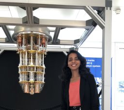 Mridula Prathapan合作论文数IBM Research Rüschlikon7Michel Despont合作论文数IBM Research Division, Zurich Research Laboratory7
 Jonathan Proesel合作论文数7
 Nikolaj Moll合作论文数Boehringer Ingelheim7Alan C Huber合作论文数7Seoyoung Jang合作论文数6matthias fertig合作论文数6
 Christoph Berger合作论文数6
 Daniel M. Kuchta合作论文数IBM T. J. Watson Research Center6thomas pflueger合作论文数5Abdullah Serdar Yonar合作论文数5