This article details the design and measurement of a digital-to-analog converter (DAC)-based source-series terminated (SST) transmitter (TX) for wireline applications in 4-nm FinFET CMOS technology. The DAC achieves 8-bit resolution and high analog output bandwidth by using a segmented architecture along with a single-ended LSB. Strength adjustment of the lower four DAC LSBs relative to the upper four DAC MSBs is accomplished with a hybrid analog/digital tuning approach, which overcomes minimum device-size limitations that can limit the effectiveness of pure digital tuning for SST drivers. The resulting DAC design achieves well-matched MSB/LSB segments with −0.63/0.67 LSB integral nonlinearity (INL) and −0.16/0.43 LSB differential nonlinearity (DNL). Time-domain modulation of 216-Gb/s PAM8 and frequency-domain modulation of 212-Gb/s orthogonal frequency-division multiplexing (OFDM) are reported, demonstrating the capability of CMOS DACs to support frequency-domain modulation for wireline applications. The TX consumes 288 mW from a 0.95-V power supply.
A 56 GS/s 8-bit asynchronous SAR ADC fabricated in 4nm CMOS technology is demonstrated. The 16x4 interleaved ADC uses a novel bootstrapping technique and a class-AB follower in the 1 st rank interleaver. It achieves a broad input common-mode (CM) range; from 0.3V to 0.6V, the total harmonic distortion stays below -52dB at 4.1 GHz with -0.2dBFS amplitude at 0.8V PPD maximum full scale. The ADC includes analog foreground calibration means for offset, gain, skew, and bandwidth. The measured ENOB is 6.5 at low frequency and stays above 5.2 up to Nyquist frequency. The bandwidth is higher than 27 GHz. The ADC uses a single 0.8V supply voltage and achieves an efficiency of 47 fJ/conv.step.
An analog-to-digital converter includes a plurality of slave sampler multiplexers responsive to outputs of a master sampler that receives analog signals and whose output ports connect to integrating threshold comparators having capacitive digital-to-analog conversion offset adjustments for forming an analog-to-thermometer code conversion. A calibration state machine receives outputs of each of the integrating threshold comparators to control the capacitive digital-to-analog conversion offset adjustment of every integrating threshold comparator and to control a calibration digital-to analog converter. A thermometer code to binary code logic decoder receives outputs of each of the integrating threshold comparators and outputs digital samples.
This paper presents a 28.05Gb/s transceiver in 32nm SOI CMOS technology. The receiver employs a quarterrate triple-speculation architecture. Techniques are introduced to adapt for mismatches in tap weights, gains and sampling phases. Error-free signaling at 28.05Gb/s is demonstrated with the transceiver over a 48dB loss backplane channel. In a four-port configuration, the power consumption at 28.05Gb/s is 484mW/lane, giving a FOM of 0.36mW/Gb/s/dB.
As CMOS devices continue to scale down in voltage and area, digital-based high-speed serial I/Os [1] become increasingly competitive with analog-based designs [2,3]. In addition to offering the PVT-independent performance of digital functions and superior power and area scaling to future technology nodes, digital-based I/Os can support advanced line modulation techniques that will become necessary as long-reach electrical channel data rates scale to 56Gb/s and beyond. The key enablers of a digital receiver are power and area efficient analog to digital conversion (ADC) and digital channel equalization. This paper describes the design of a 25Gb/s 2-level digital serial line receiver including a ¼-rate 5b flash ADC, an 8-tap feed-forward equalizer (FFE), an 8-tap decision-feedback equalizer (DFE), and a baud-rate clock and data recovery circuit (CDR). The receiver features a flash ADC, which employs a new power and area efficient slicer design capable of achieving high-precision (∼1mV) threshold accuracy with an associated on-chip calibration system. The 32nm SOI CMOS receiver achieves error-free operation with margin on a reflective transmission-line channel with 40dB half-baud loss.
This paper describes key design features of a 32 Gb/s 4-tap FFE/15-tap DFE transceiver in 32 nm SOI CMOS which mitigate major sources of degradation in transceiver performance. The transceiver employs a passive feed-forward restore (FFR) scheme in an on-chip AC-coupling network to prevent pattern-dependent baseline wander, a low-latency clock and data recovery (CDR) to improve high-frequency jitter tolerance, and a token-based power management scheme to reduce supply ripple. At 32 Gb/s, the transceiver can equalize a channel with 30 dB of loss at a bit-error rate below 10 -12 while consuming 21 mW/Gbps at 1 V supply and an area of 0.7 mm 2 .
In this paper, we present a digital equalizer for 16Gb/s backplane I/Os which consumes only 3.5pJ/bit for an 8-tap FFE and 4+4 tap DFE operation. Several design choices were chosen to enable low power consumption at high speed. First, the FFE leverages parallelism to lower the supply voltage, while the DFE runs from a higher supply to close the feedback loop. Second, the FFE uses distributed arithmetic to reduce the number of required additions. Third, the DFE taps leave a window of four equalizer taps, which are covered by the FFE, in order to close the timing. Finally, a custom digital design style was chosen, which enabled the optimization of critical blocks and wires. At 0.6V supply, the FFE was measured to consume 1pJ/bit, while the DFE consumes 1.6pJ/bit at 0.9V while running at 16Gb/s.
A low-power receiver circuit in 32 nm SOI CMOS is presented, which is intended to be used in a source-synchronous link configuration. The design of the receiver was optimized for power owing to the assumption that a link protocol enables a periodic calibration during which the circuit does not have to deliver valid data. In addition, it is shown that the transceiver power and the effect of high-frequency transmit jitter can be reduced by implementing a linear equalizer only on the receive side and avoiding a transmit feed-forward equalizer (TX-FFE). On the circuit level, the receiver uses a switched-capacitor (SC) approach for the implementation of an 8-tap decision-feedback equalizer (DFE). The SC-DFE improves the timing margin relative to previous DFE implementations with current feedback, and leads to a digital-style circuit implementation with compact layout. The receiver was measured at data rates up to 13.5 Gb/s, where error free operation was verified with a PRBS-31 sequence and a channel with 32 dB attenuation at Nyquist. With the clock generation circuits amortized over eight lanes, the receiver circuit consumes 2.6 mW/Gbps from a 1.1 V supply while running at 12.5 Gb/s.
This paper presents a 28-Gb/s transceiver in 32-nm SOI CMOS technology for chip-to-chip communications over high-loss electrical channels such as backplanes. The equalization needed for such applications is provided by a 4-tap baud-spaced feed-forward equalizer (FFE) in the transmitter and a two-stage peaking amplifier and 15-tap decision-feedback equalizer (DFE) in the receiver. The transmitter employs a source-series terminated (SST) driver topology which doubles the speed of existing half-rate designs. The high-frequency boost provided by the peaking amplifier is enhanced by adopting a structure with capacitively coupled parallel input stages and active feedback. A capacitive level-shifting technique is introduced in the half-rate DFE which allows a single current-integrating summer to drive the four parallel paths used for speculating the first two DFE taps. Error-free signaling at 28 Gb/s is demonstrated with the transceiver over a channel with 35 dB loss at half-baud frequency. In a four-port core configuration, the power consumption at 28 Gb/s is 693 mW/lane.
As exemplified by standards such as OIF CEI-25G, 32G-FC, and next-generation 100GbE, serial link data rates are being pushed up to 25 to 28Gb/s in order to increase I/O system bandwidth. Such speeds represent a near doubling of the state-of-the-art for fully integrated transceivers [1-3]. With scaling no longer providing large gains in device speed, significant design advances must be made to attain these data rates. This paper describes a 28Gb/s serial link transceiver featuring a source-series terminated (SST) driver topology with twice the speed of existing designs, a two-stage peaking amplifier with capacitively-coupled parallel input stages and active feedback, and a 15-tap DFE. The use of capacitive level-shifters allows a single current-integrating summer to drive the parallel paths used for speculating the first two DFE taps.
This paper presents a 16-Gb/s 45-nm SOI CMOS transceiver for multi-standard backplane applications. The receiver uses a 12-tap DFE with circuit refinements for supporting higher data rates. Both the receiver and the transmitter use dynamic adaptation to combat parameter drift due to changing supply and temperature. A 3-tap FFE is included in the source-series-terminated driver. The combination of DFE and FFE permits error-free NRZ signaling at 16-Gb/s over channels exceeding 30dB loss. The 8-port core with two PLLs is fully characterized for 16GFC and consumes 385 mW/link.
 scott k reynolds合作论文数18
 Brian Floyd合作论文数Department of Electrical and Computer Engineering, North Carolina State University17
 Brian P Gaucher合作论文数Thomas J Watson Res Ctr, IBM Corp13
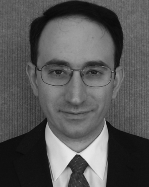 John F. Bulzacchelli合作论文数IBM T. J. Watson Research Center10
 Ullrich Pfeiffer合作论文数Lehrstuhl für Hochfrequenzsysteme in der Kommunikationstechnik, Bergische Universität Wuppertal10
 Sergey V. Rylov合作论文数ibm9
 Alberto Valdes Garcia合作论文数Thomas J. Watson Research Center, IBM Research8
 Mounir Meghelli合作论文数Mixed Signal Communication IC Design Group, IBM T.J. Watson Research Center8
 Michael P. Beakes合作论文数IBM T. J. Watson Research Center8
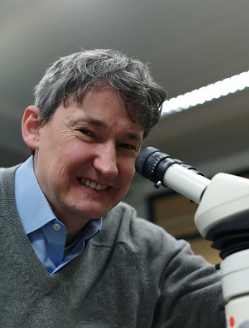 Thomas Toifl合作论文数Cisco Systems8Herschel A. Ainspan合作论文数8william r kelly合作论文数7
 Chuck Haymes合作论文数7
 Marcel Kossel合作论文数IBM Research - Zurich7
 Michael a Sorna合作论文数6
 Matthias Braendli合作论文数IBM Zürich Research Laboratory6
 Peter Buchmann合作论文数6
 Janusz Grzyb合作论文数IHCT, Bergische Univ.;c;IHCT, Bergische Univ.5
 Zeynep Toprak Deniz合作论文数IBM T.J. Watson Research Center5
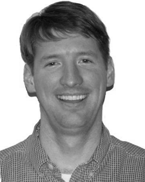 Daniel W. Storaska合作论文数5
 Thomas Morf合作论文数IBM Research – Zurich5
 Duixian Liu (刘兑现)合作论文数IBM T. J. Watson Research Center5
 Pier Andrea Francese合作论文数IBM Zurich Research Laboratory5
 Thomas Zwick合作论文数Institut für Hochfrequenztechnik und Elektronik, Karlsruher Institut für Technologie5karl d selander合作论文数4
 Daniel J. Friedman合作论文数National Renewable Energy Laboratory4Scott K Reynolds合作论文数4
 Mehmet Soyuer合作论文数IBM Thomas J. Watson Research Center4
 Andrea Prati合作论文数Dipartimento di Ingegneria e Architettura, Università degli studi di Parma;Department of Information Engineering, Università degli Studi di Parma4
 Gautam R. Gangasani合作论文数4
 Christian Menolfi合作论文数Cisco Systems4
 Daniele Gardellini合作论文数4
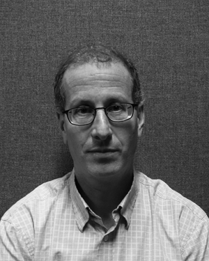 Jon Garlett合作论文数4
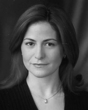 Benjamin D. Parker合作论文数4
 Hui H. Xu合作论文数3
 Christian Baks合作论文数3
 Alexander Rylyakov合作论文数Nokia3Yong Liu合作论文数Shanghai Jiao Tong University3
 Woogeun Rhee (李宇根)合作论文数School of Integrated Circuits, Tsinghua University3
 Daiju Nakano合作论文数IBM Research - Tokyo3
 Young-Je Kwark合作论文数Department of Organic Materials and Fiber Engineering, Soongsil University3
 Chun-Ming Hsu合作论文数Kuang Tien General Hospital3Hyo-Gyuem Rhew合作论文数2Michael Wielgos合作论文数2
 Matthew Baecher合作论文数2
 Hyoungbae Ahn合作论文数2Vivek Sharma合作论文数2
 Young-Ho Choi合作论文数Samsung Electronics, Hwaseong, Korea#TAB#2
 Gunil Kang合作论文数Samsung Electronics, Hwaseong, Korea#TAB#2




