Aggressive gate pitch scaling makes it increasingly challenging to control the doping gradient at the source/drain (S/D) extensions. To address this, S/D underlap doping has been proposed as a solution. However, anomalous I-D,I-lin saturation has been experimentally observed in such devices, raising questions about its physical origin. In this work, we investigate the transport physics in ultra-scaled nanosheet FETs by solving the Subband Boltzmann Transport Equation. The simulation results reveal that secondary barriers formed in underdoped S/D extensions enhance quasi-ballistic transport even in the linear regime, providing a consistent explanation for the observed I-D,I-lin saturation in underlap devices. These insights offer guidance for optimizing S/D underlap doping profiles, highlighting the need to avoid excessive Gate-S/D overlap capacitance while preventing on-current degradation.
Contacted-poly-pitch (CPP) scalability of gate-all-around (GAA) nanosheet (NS) device is investigated in detail. Combination of NS thickness (TNS) and junction abruptness (delta) allow for spacer thickness (T-SP) and gate-length (L-G) scaling. Contact-length L-CNT scaling does not affect intrinsic performance, but scaling is limited by middle-of-line and interface resistivity. Using an extensively calibrated advanced transport model combined with the transistor design-technology co-optimization (DTCO) flow we account for accurate device and circuit intrinsics and parasitics. We highlight the trade-off between T-SP and L-G scaling whereby L-G can be scaled more aggressively if T-SP can be relaxed. T-NS can be scaled to-3.5 nm maintaining iso-performance allowing for a minimum CPP of-38 nm at L-G 10 nm. Aggressively improving delta- can further allow CPP scaling to-34 nm (L-G similar to 6 nm), though T-NS scaling gain saturates due to severe transport degradation.
Using a full design-technology-co-optimization (DTCO) methodology, we show the advantages of design decoupling of inner -and outer-gates in gate-all-around nanosheet FETs. Trade-off between short-channel effects (SSAT), external resistance (REXT), effective capacitance (CEFF including parasitic capacitance CPARA) favors for a more aggressive outer-LG scaling (reduces CPARA and/or relaxes contact length, LCNT) keeping inner-LG relaxed (controls REFF, SSAT). Up to 10% speed-at-iso-leakage and speed-at-iso-power, and 15% power-at-iso-speed gains are possible with this unique design available in GAA-NS based devices, allowing for multi-node GAA extension without scaling more fundamental geometry parameters like thickness of NS.
Amorphous indium gallium zinc oxide (a-IGZO) is becoming an increasingly important technological material. Transport in this material is conceptualized as the heavy disorder of the material causing a conduction or mobility band-edge that randomly varies and undulates in space across the entire system. Thus, transport is envisioned as being dominated by percolation physics as carriers traverse this varying band-edge landscape of “hills” and “valleys”. It is then something of a missed opportunity to model such a system using only a compact approach—despite this being the primary focus of the existing literature—as such a system can easily be faithfully reproduced as a true microscopic TCAD model with a real physically varying potential. Thus, in this work, we develop such a “microscopic” TCAD model of a-IGZO and detail a number of key aspects of its implementation. We then demonstrate that it can accurately reproduce experimental results and consider the issue of the addition of non-conducting band-tail states in a numerically efficient manner. Finally, two short studies of 3D effects are undertaken to illustrate the utility of the model: specifically, the cases of variation effects as a function of device size and as a function of surface roughness scattering.
Ferroelectric memory devices have seen intense interest over the last decade. However, in heavily scaled devices such as silicon-on-insulator (SOI), FinFETs, and nanowire-based FETs the observed ferroelectric memory window (MW) is heavily degraded owing to the fact that additional majority carriers cannot be sourced as there is no "bulk." Thus, the device never enters accumulation and polarization switching is suppressed due to the semiconductor channel remaining depleted. Here, we promote an ambipolar Schottky-based ferroelectric transistor (AS-FeFET) as an alternative design. We demonstrate that such devices-owing to their ambipolar nature and thus the ability to source both types of carriers-exhibit MWs that are consistently $\sim$ 40%-60% larger than conventional devices for the same programming conditions. Although these devices do suffer from a reduced ON-current, this tradeoff remains very attractive for many applications.
This multi-partner-project contribution introduces the midway results of the Horizon 2020 FVLLMONTI project. In this project we develop a new and ultra-efficient class of ANN accelerators, the neural network compute cube ((NC2)-C-2), which is specifically designed to execute complex machine learning tasks in a 3D technology, in order to provide the high computing power and ultra-high efficiency needed for future edgeAI applications. We showcase its effectiveness by targeting the challenging class of Transformer ANNs, tailored for Automatic Speech Recognition and Machine Translation, the two fundamental components of speech-to-speech translation. To gain the full benefit of the accelerator design, we develop disruptive vertical transistor technologies and execute design-technology-co-optimization (DTCO) loops from single device, to cell and compute cube level. Further, a hardware-software-co-optimization is executed, e.g. by compressing the executed speech recognition and translation models for energy efficient executing without substantial loss in precision.
Complimentary FETs (CFETs) enable aggressive standard cell height (CH) reduction, facilitating on-target area scaling without shrinking contacted gate pitch (CGP). We extensively benchmark nanosheet (NS) based CFETs against gate-all-around (GAA) NSFETs using power, performance, area (PPA) as well as scalability metrics. The impact of BEoL RC, new materials, DTCO boosters is further explored. 4T CFET designed with 20 nm metal pitch (MP) offers 62% smaller area and 28% extra speed at iso-power over reference NS devices.
We present TCAD-based methodologies that go beyond process and device simulations of single transistors. We show that TCAD solvers can be used as effective tools to resolve the intricacies of current and future technology nodes that are otherwise difficult to access using EDA-level methods alone.
We present a hierarchical flow for predictive TCAD device simulation in DCTO applications. Using a thoroughly cal-ibrated sub-band Boltzmann transport equation (SBTE) solver, TCAD device simulation parameters for the technology under investigation are generated automatically. This flow enables predictive accuracy of the SBTE solver at turn-around-times of SPICE simulations. It is demonstrated here for an A14 nanosheet technology, i) showing all intermediate calibration details and ii) highlighting a considerable improvement in the accuracy of ring-oscillator performance.
Advancements in the semiconductor industry introduce novel channel materials, device structures, and integration methods, leading to intricate physics challenges when characterizing devices at circuit level. Nevertheless, accurate models for emerging devices are crucial for physics-driven TCAD-to-SPICE flows to enable the increasingly vital design technology co-optimization (DTCO). Particularly for ultra-scaled devices where quantum effects become significant, this led to the introduction of empirical model parameters and a disconnection to manufacturing processes. To catch up with these developments, an alternative to the traditional white-box modeling methods has attracted much attention: machine learning-assisted compact modeling (MLCM). These black-box methods target towards general-purpose modeling of complex mathematics and physics through training of neural networks on experimental and simulated data, generating an accurate closed-form mapping between output characteristics and input parameters for fabrication process and device operation. To address this new trend, this work provides a comprehensive overview of emerging device model methodologies, spanning from device physics to machine learning engines. By analyzing, structuring, and extending distributed efforts on this topic, it is shown how MLCM can overcome limitations of traditional compact modeling and contribute to effective DTCO to further advance semiconductor technologies.
Process technology computer aided design (TCAD) has become an indispensable tool to characterize proposed future technologies. However, current solutions often require tedious manual calibrations of process flows. Here, we present the automatic processing of electron microscopy (EM) images to 2D and 3D device representations. Parts of the device which are not present in the EM image are emulated to create a structure ready for device simulation. The feasibility of this approach is shown by extracting the fin shape from the EM image of a 7nm FinFET, as well as studying the impact of fin shape on device characteristics in an exemplary variability study. Additionally, the inner spacers and gate shape of a nanosheet (NS) FET are reproduced, showcasing the applicability of the presented approach to different device technologies.
Using a full device-technology-co-optimization (DTCO) methodology, we show the advantages of design decoupling of inner $\left(\mathrm{L}_{\mathrm{G}(\mathrm{I})}\right)$- and outer $\left(\mathrm{L}_{\mathrm{G}(\mathrm{O})}\right)$- gates in gate-all-around nanosheet FETs. A better trade-off between short-channel effects ($\mathrm{S}_{S A T}$), external resistance $\left(\mathrm{R}_{\mathrm{EXT}}\right)$, effective favors for a more aggressive $\mathrm{L}_{G(O)}$ scaling (reduces C CARA and/or relaxes contact length, $\mathrm{L}_{\mathrm{CNT}}$) keeping $\mathrm{L}_{\mathrm{G}(\mathrm{I})}$ relaxed (controls $\mathrm{R}_{\mathrm{EFF}}, \mathrm{S}_{\mathrm{SAT}}$). Up to 10% speed-at-iso-leakage, 11% speed-at-iso-power, and 15% power-at-iso-speed gains are possible with this design, in addition to allowing better contact-poly pitch (CPP) scaling path.
In this work a TCAD model of a ferroelectric VNAND device is developed and validated against experimental data. After its accuracy is demonstrated it is then used to explore a number of issues related to the future potential of such devices including: the expected performance if negative trapping effects are reduced, the variability issues created by the polyphasic nature of hafnium-based ferroelectric films, the issue of the destructive nature of the read sweep, and poor effect of ERS pulses. In addition, some mitigation strategies to combat these issues are briefly discussed.
Ferroelectric-based transistors (FeFETs) are an important emerging technology with applications both as conventional memories and in emerging computational paradigms such as in-memory, neuromorphic and edge computing. A common modeling approach in these structures is to treat the system as a Metal-Ferroelectric-Insulator-Semiconductor (MFIS) effective circuit and use this to both qualitatively and quantitatively model device behavior. However, such approaches completely ignore three-dimensional effects. In this work TCAD is used to conduct three case studies meant to highlight common situations where a non-3D-modeling approach will lead to markedly incorrect predictions of device behavior. These three cases are: 1) channel percolation effects, 2) non-unixial ferroelectricity and 3) geometric depletion effects in SOI, Gate-All-Around (GAA) and nanowire devices. Finally, as a counter-case the observed steep-subthreshold in FeFETs has been argued to be a 3D percolation effect but here it is demonstrated that such behavior is present within an MFIS approach as well.
We examine the dependence of source-to-drain tunneling (SDT) leakage on the effective channel length (L eff ) for Si and Ge pMOS with L eff ranging from 5 nm to 20 nm. The subband Boltzmann transport equation is solved including the SDT process, which is evaluated from the WKB approximation. Device architectures including nanosheet transistors (NSTs) and nanowire transistors (NWTs) with the proper specification are analyzed. The results show that SDT becomes a serious concern for Ge pNSTs with L eff lower than 17 nm. However, such leakage degradation from SDT, can be further mitigated by optimizing the cross-sectional configuration.
A novel DTCO flow is described with the principal aim to study the impact of air spacer fabrication on the power and performance of a 5-stage inverter ring oscillator at the 7 nm node. The flow incorporates physical and analytical process models from the in-house ViennaPS simulation tool together with device and circuit simulations from GTS Framework's Cell Designer. The air spacer is usually filled by sequential conformal and non-conformal deposition steps. The impact of the thickness of the conformal layer and the sticking probability during non-conformal deposition on the ring oscillator performance is studied here. The air gap, which forms the core of the air spacer, is generated during the non-conformal deposition step. We extract the relative effective permittivity of the air spacer as a function of these two fabrication parameters by solving the Poisson equation to obtain the spacer capacitance. Finally, SPICE model cards are extracted automatically from the TCAD transistor characteristics and the parasitic network is calculated from the full 3D ring oscillator logic cell using a field solver. We apply our framework on two fabrication flows, when the air gap is created before and after the deposition of the first metal contacts layer. We observe that introducing the air gap inside the spacer results in an at-least 15% improvement in the ring oscillator's performance, when the power is kept constant. Further improvements can be achieved by reducing the conformal layer thickness and increasing the sticking probability by increasing the chamber partial pressure or increasing the process temperature.
In this preprint we present a novel approach to solving the transport problem in semiconductors. We reformulate the drift-diffusion equations in terms of the quasi-Fermi-energies as solution variables; a drastic increase in numerical stability is achieved, which permits the simulation of devices at cryogenic temperatures as well as wide-band-gap devices using double precision arithmetic, instead of extended precision arithmetic which would otherwise be required to solve these applications using regular drift-diffusion.
Ultra-wide (UW) optical coherence tomography angiography (OCTA) imaging provides new opportunities for diagnosing medical diseases. To further support doctors in the recognition of diseases, automated image analysis pipelines would be helpful. Therefore the MICCAI DRAC 2022 challenge was carried out, which provided a standardized UW (swept-source) OCTA data set for testing the effectiveness of various algorithms on a diabetic retinopathy (DR) dataset. Our team tried to train well-performing segmentation models for UW-OCTA analysis and was finally ranked under the three top-performing teams for segmenting DR lesions. This paper, therefore, summarizes our proposed strategy for this task and further describes our approach for image quality assessment and DR Grading.
We present a novel approach to the modeling of carrier energy relaxation during high-field phases in semiconductor-oxide-nitride-oxide-semiconductor (SONOS) flash memory gate stacks. We show that this method integrates well with TCAD simulators and that taking the energy relaxation of carriers into consideration solves two of the most prominent problems of trapping layer dynamics modeling: The missing slope degradation in incremental step-pulse programming (ISPP) simulations and the incompatibility of the resulting charge distributions with long-term room temperature charge retention measurements. This article consists of two parts where this part discusses the physical/TCAD level. The second part derives a semianalytical model specifically for programming that reduces the numerical complexity while still retaining the main physical assumptions and the applicability to experimental data.
 Zlatan Stanojevic合作论文数Institute for Microelectronics, TU Wien62
 Oskar Baumgartner合作论文数Institute for Microelectronics, TU Wien51
 Ch. Kernstock合作论文数31
 Franz Schanovsky合作论文数Christian Doppler Laboratory26
 Tibor Grasser合作论文数Institute for Microelectronics, Technische Universität Wien24
 Gerhard Rzepa合作论文数22f mitterbauer合作论文数16H Kosina合作论文数14
 Hans Kosina合作论文数14
 Siegfried Selberherr合作论文数Institute for Microelectronics, Technische Universitat Wien9
 Martin Vasicek合作论文数9G. Strof合作论文数8h demel合作论文数8H. W. Karner合作论文数7
 Wolfgang Goes合作论文数7
 Antonio Arreghini合作论文数7
 Holzer, S.合作论文数7
 Mischa Thesberg合作论文数Department of Physics and Astronomy, McMaster University7Georg Strof合作论文数6
 Ben Kaczer合作论文数Imec6
 Devin Verreck合作论文数6Martin Wagner合作论文数6
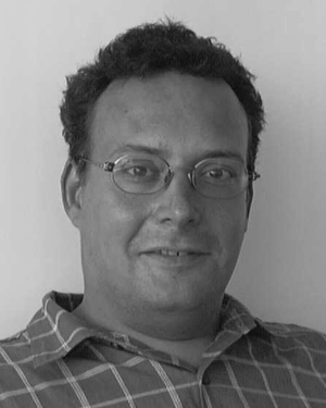 Johann Cervenka合作论文数TU Wien Institute for Microelectronics6La Filipovic合作论文数5Christian Kernstock合作论文数5
 A. Gehring合作论文数5
 G. Van Den Bosch合作论文数5
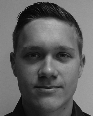 Xaver Klemenschits合作论文数4
 Thomas Mikolajick合作论文数Center for Advancing Electronics Dresden, Dresden University of Technology4
 Edward F. DeLong合作论文数Department of Oceanography, School of Ocean and Earth Science and Technology, University of Hawaii4
 Maarten Rosmeulen合作论文数4
 Jens Trommer合作论文数NaMLab gGmbH, Dresden, Germany4
 Krishna Kumar Bhuwalka合作论文数tsmc4
 Changze Liu合作论文数Inst Microelect, Peking Univ4Chen-Ming Tsai合作论文数3
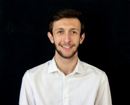 L. Reveil合作论文数3
 Jose Maria Gonzalez-Medina合作论文数Global TCAD Solutions GmbH3S. Holzer合作论文数3Hao Wu合作论文数3
 Furnemont, Arnaud合作论文数3Hajdin Ceric合作论文数3
 Dmitry Yakimets合作论文数Imec;c;Imec3
 Chhandak Mukherjee合作论文数3
 Cedric Marchand合作论文数Lab. Hubert Curien, Univ. of Lyon;c;Lab. Hubert Curien, Univ. of Lyon3
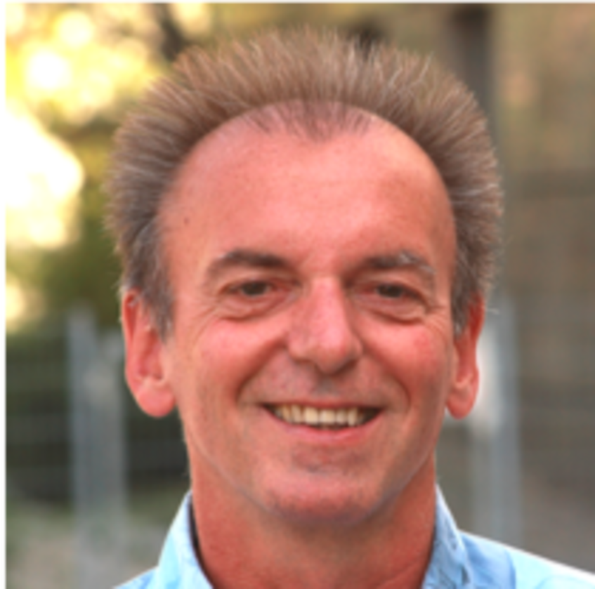 Gerhard J. Herndl合作论文数Department of Functional and Evolutionary Ecology,
University of Vienna;Royal Netherlands Institute for Sea Research3
Gerhard J. Herndl合作论文数Department of Functional and Evolutionary Ecology,
University of Vienna;Royal Netherlands Institute for Sea Research3 David M. Karl合作论文数Department of Oceanography, School of Ocean and Earth Science and Technology, University of Hawai‘i at Manoa;Daniel K. Inouye Center for Microbial Oceanography, University of Hawai‘i at Manoa3M. Wagner合作论文数3
 Ian O’Connor合作论文数3
 David Atienza Alonso合作论文数Embedded Systems Laboratory, École Polytechnique Fédérale de Lausanne;Institute of Electrical and Micro Engineering, École Polytechnique Fédérale de Lausanne3




