The semiconductor revolution in automobiles is currently driven by drive train electrification and autonomous driving (ADAS). Powered by engineered substrates, FD-SOI, with its unique features of low power/leakage, back bias and excellent RF performance, is well positioned for this. Engineered substrate innovations can prepare FD-SOI to meet the future demands like next generation automotive radars, and a substrate aware PDK helps match the right substrate innovation to the right application.
A near-threshold power supply aims to operate at the minimal energy point but suffers from high-sensitivity to process, temperature and voltage variations. Adaptive voltage scaling (AVS) is a well-known strategy to adapt the power supply to die-to-die and temperature variations [1]. However, AVS needs dedicated power supplies with nonnegligible overheads, e.g. extra die area, lower power converter efficiency, and with granularity limitations or complex fine-grain integration in the power mesh. SOI-based technologies offer unique features by biasing the wells below the transistors to tune the threshold voltage (V TH ). The well-known adaptive back-biasing (ABB) technique has already shown its capability to reduce power consumption or/and maintain operating frequency by compensating V TH variability according to process corners and temperature [1-5]. However, previously published ABB architectures provide a limited overview on how to integrate the ABB seamlessly in the digital design flow with industrial-grade qualification. We propose a reusable ABB-IP for any biased digital load, from 0.4-100 mm 2 , with low area and power overhead, e.g. 1.2% @ 2mm 2 and 0.4% @ 10mm 2 , respectively. We properly quantify the gain in a mass-production context with a large statistical scope analysis across 316 measured dies from different split-wafer lots and from -40 to 125°C with a representative load (a Cortex M4F). Thanks to 3V asymmetrical wells amplitude swing, our ABB-IP brings up to 30% power reduction by decreasing the minimal power supply by 100mV, while maintaining the target operating frequency (50 MHz) with a high yield. Distributed timing monitors (DTM) guarantee an accurate timing monitoring of the biased digital load, while scalable well drivers adjust to the biased well area, enabling the ABB-IP genericity.
The performance and reliability of Ultra-Low-Power (ULP) computing platforms are adversely affected by environmental temperature and process variations. Mitigating the effect of these phenomena becomes crucial when these devices operate near-threshold, due to the magnification of process variations and to the strong temperature inversion effect that affects advanced technology nodes in low-voltage corners, which causes huge overhead due to margining for timing closure. Supporting an extended range of reverse and forward body-bias, UTBB FD-SOI technology provides a powerful knob to compensate for such variations. In this work we propose a methodology to maximize energy efficiency at run-time exploiting body biasing on a ULP platform operating near-threshold. The proposed method relies on on-line performance measurements by means of Process Monitoring Blocks (PMBs) coupled with an on-chip low-power body bias generator. We correlate the measurement performed by the PMBs to the maximum achievable frequency of the system, deriving a predictive model able to estimate it with an error of 9.7% at 0.7 V. To minimize the effect of process variations we propose a calibration procedure that allows to use a PMB model affected by only the temperature-induced error, which reduces the frequency estimation error by 2.4x (from 9.7% to 4%). We finally propose a controller architecture relying on the derived models to automatically regulate at run-time the body bias voltage. We demonstrate that adjusting the body bias voltage against environmental temperature variations leads up to 2X reduction in the leakage power and a 15% improvement on the global energy consumption when the system operates at 0.7 V and 170 MHz.
Improving the energy efficiency of processor systems-on-chip (SoCs) is key to improving their performance and utility. The FD-SOI silicon process enables integrated systems that can deliver dramatic improvements in energy efficiency through system integration. This chapter presents the Raven-3 and Raven-4 testchips, fully integrated and fully featured SoCs which achieve energy-efficient operation with low overhead. RISC-V processors allow for innovation and experimentation in the context of a free, open architecture. Integrated switched-capacitor voltage regulators can achieve high conversion efficiency when coupled with adaptive clock generators. Custom SRAM macros operate at low supply voltages, enabling wide voltage scaling. An integrated body-bias generator allows run-time tuning of threshold voltage for improved performance or reduced leakage. Taken together, these innovations showcase the possibilities of FD-SOI technology.
This paper unveils a new methodology for defining the characterization corners for standard cells, memories or any hard macros for their use in conjunction with an adaptive body bias control loop system. The objective is to define the optimum body bias values that maximize the speed performance of a digital macro without degrading its power consumption by analyzing the transistor behavior among process, voltage and temperature variations. The proposed methodology developed for the 22FDX technology from GLOBALFOUNDRIES demonstrates significant performance gains over the full voltage range of the technology wrt any other compensation techniques.
This work demonstrates that up to 74% energy efficiency can be gained by combining Body-Bias Process, Temperature and Aging compensation schemes altogether. This combination of compensation schemes offers the best energy efficiency gain as compared to recent results while guaranteeing high-level of robustness (<;1 ppm) and safety for automotive products.
Worst-case design and post-silicon tuning are well established digital design practices reducing timing violations in presence of process, temperature, aging and voltage variations, but they suffer from extra power consumption due to overdesign [1]. Adaptive voltage scaling (AVS) [2] and body bias modulation [1] are well-known strategies to dynamically ensure that the digital core can operate at a targeted frequency, even in the presence of delay degradation due to variations. In a multiple voltage islands context, AVS requires many integrated supply generators, such as switched capacitor converters that need to be controlled accurately. Also, for fine-grained compensation, level shifters are required, impacting circuit performance. As FDSOI technology offers the ability to adjust transistor speed through high sensitivity (85mV/V BB ) V TH tuning by acting on buried Nwell (NW) and Pwell (PW) voltages, back-biasing generators have been investigated [3-5]. However, they require an external controller to reach the optimal Back Bias (BB) voltages (no self-adjustment) ([3-4] and [5]), imposing a non-negligible area overhead for a sub-mm 2 digital core having a narrow compensation range limited to 0.35-0.45V V DD . We therefore propose a variation-aware BB compensation unit (BBC), which dynamically self-adjusts the N- and PMOS transistors' BB voltages to maintain the target frequency with low-latency tuning (100μs) across a wide range of supply voltage (0.35-1V) and temperature (-40-125°C). The low reported area of 0.0067mm 2 makes it affordable for a small digital core area (0.1-2mm 2 ). Requiring only a reference frequency signal F TGT , the self-operating BBC exhibits 2.5μW quiescent current without any external components. Compared to a worst-case design strategy, the BBC unit brings up to 50% leakage reduction @0.45V DD , 120°C and reduces the energy per cycle up to 32% compared to worst-case design. By providing continuous BB voltage adjustment (continuous V TH tuning), the target frequency is maintained within ±3.5% accuracy.
Advanced Ultra-Low Power (ULP) computing platforms can be affected by large performance variations. This phenomenon is mainly caused by process and ambient temperature variations, and it is magnified by the strong Temperature Effect Inversion (TEI) that characterizes devices when operating Near-Threshold (NT) in highly scaled nodes. 28nm UTBB FD-SOI technology supports an extended range of both forward and reverse Body-Bias (BB) voltage. This feature can be efficiently used to reduce margins at design time and compensate variations at runtime. In this paper we propose a BB voltage controller capable to independently probe the maximum frequency of P and N transistors, and leverage a BB voltage adjustment to achieve a user-specified target frequency, minimizing the leakage current. Compared to the case where zero BB is applied to the transistors, the controller achieves up to 23% power reduction exploiting the performance increase originated by TEI, further reducing power by 12% with respect to a symmetric BB approach.
Energy efficiency is a crucial aspect in modern SoCs. Common strategies like aggressive voltage scaling and parallel processing have enabled major improvements in active energy efficiency. However, the big impact of process variations, as well as the temperature sensitivity of devices operating in near threshold force digital designers to adopt very conservative margins for timing closure.
Fully depleted silicon-on-insulator (FD-SOI) devices built on an ultrathin SOI layer on a buried-oxide (BOX) substrate feature unique performance capabilities and are suitable for full-range body biasing. FD-SOI technology has been adopted for multiple technology nodes and a wide range of current and upcoming microelectronic market segments, especially in the Internet of Things (IoT), wearable ele...
Polar codes are a recently proposed class of block codes that provably achieve the capacity of various communication channels. They received a lot of attention as they can do so with low-complexity encoding and decoding algorithms, and they have an explicit construction. Their recent inclusion in a 5G communication standard will only spur more research. However, only a couple of ASICs featuring decoders for polar codes were fabricated, and none of them implements a list-based decoding algorithm. In this paper, we present ASIC measurement results for a fabricated 28-nm CMOS chip that implements two different decoders: the first decoder is tailored toward error-correction performance and flexibility. It supports any code rate as well as three different decoding algorithms: successive cancellation (SC), SC flip, and SC list (SCL). The flexible decoder can also decode both non-systematic and systematic polar codes. The second decoder targets speed and energy efficiency. We present measurement results for the first silicon-proven SCL decoder, where its coded throughput is shown to be of 306.8 Mbps with a latency of 3.34 us and an energy per bit of 418.3 pJ/b at a clock frequency of 721 MHz for a supply of 1.3 V. The energy per bit drops down to 178.1 pJ/b with a more modest clock frequency of 308 MHz, lower throughput of 130.9 Mbps and a reduced supply voltage of 0.9 V. For the other two operating modes, the energy per bit is shown to be of approximately 95 pJ/b. The less flexible high-throughput unrolled decoder can achieve a coded throughput of 9.2 Gbps and a latency of 628 ns for a measured energy per bit of 1.15 pJ/b at 451 MHz.
As technology edges closer to fundamental limits, variations of process parameters, operational voltage, and temperature (PVT variations) have to be accounted for. This paper proposes to make higher levels aware of these variations and bring them under system control by using software controlled body biasing. PVT variations can thus be exploited to reduce power and energy consumption.—Axel Jantsch...
Reconfigurable finite-impulse response (FIR) filters are one of the most widely implemented components in Internet of Things systems that require flexibility to support several target applications while consuming the minimum amount of power to comply with the strict design requirements of portable devices. Due to the significant power consumption in the multiplier components of the FIR filter, various techniques aimed at reducing the switching activity of these multipliers have been proposed in the literature. However, these techniques rarely exploit the flexibility on the algorithmic level, which can lead to additional benefits. In this paper, FIR filter multipliers are extensively characterized with power simulations, providing a methodology for the perturbation of the coefficients of baseline filters at the algorithm level to trade-off reduced power consumption for filter quality. The proposed optimization technique does not require any hardware overhead and it enables the possibility of scaling the power consumption of the filter at runtime, while ensuring the full baseline performance of any programmed filter whenever it is required. The analyzed FIR filters were fabricated in a 28nm FD-SOI test chip and measured at a near-threshold, 600mV supply voltage. For example, by carefully choosing slightly perturbed coefficients in a low-pass configuration, power savings of up to 33% are achieved when accepting a 3dB degradation on the stopband, as compared with the baseline implementation of the filter.
In this paper, a built-in Body Bias design methodology is proposed and implemented in two different contexts: the automotive industry and the IoT paradigm. As opposed to the traditional design strategy, the proposed methodology incorporates Body Bias in all design stages, from synthesis to engineering. Measurements performed in a leakage-driven ADAS product and a dual core application processor in 28nm UTBB-FDSOI technology confirm the effectiveness of the proposed methodology, achieving a 30% reduction in static power, 25% in dynamic power, 15% yield recovery, and a 4X frequency and 2X leakage spread reduction.
This article presents an ultra-low-power parallel computing platform and its system-on-chip (SoC) embodiment, targeting a wide range of emerging near-sensor processing tasks for Internet of Things (IoT) applications. The proposed SoC achieves 193 million operations per second (MOPS) per mW at 162 MOPS (32 bits), improving the first-generation Parallel Ultra-Low-Power (PULP) architecture by 6.4 and 3.2 times in performance and energy efficiency, respectively.
This paper presents a comprehensive analysis of Adaptive Body Bias (ABB) interests provided by Fully Depleted Silicon On Insulator (FDSOI) technology. At transistor level, we demonstrate a total process variability and temperature effect compensation thanks reverse and forward bias. Those benefits have been reached without degradation of devices reliability versus regular Adaptative Voltage Scaling solution (AVS). Leveraging this triple advantages (variability, temperature and ageing), digital design density is discussed showing significant reduction of W/L metric in case of ABB usage in CPU core. Forward Body Biasing (FBB) exhibited significant analog performance increasing (+100%) on key parameters such as gm and gd for both I/Os and core oxide devices. Finally, outstanding Vmin yield improvement thanks to ABB technique is demonstrated on commercial product in the automotive market.
An optimized co-design of SRAM cell, assist schemes, and layout is proposed to achieve wide voltage range operation of SRAM from 0.35-1.2 V at all process corners. A differential read asymmetric 8 T memory cell and a data dependent differential supply and body modulation write assist scheme are proposed. We also propose a layout that reduces metal capacitance of wordlines by 54% and also enables bit-interleaving. The proposed assist scheme can be combined with conventional assist schemes to further lower minimum write operational voltage of the SRAM by 70-130 mV at iso-performance without causing reliability concerns. A 32 kb instance is fabricated in 28-nm UTBB-FDSOI technology and efficiency of the proposed scheme is demonstrated with lowest write voltage of 0.32 V. Multiple read assist schemes have been used to simultaneously lower read voltage to 0.35 V. 50 MHz operation is measured when integrated in a DSP processor at 0.358 V. Low voltage and wide voltage range figure of merits are also defined to benchmark the proposed solutions with other works.
Low power (mW) and high performance (GOPS) are strong requirements for compute-intensive signal processing in E-health, Internet-of-Things, and wearable applications. This work presents a building block for programmable Ultra-Low Power accelerators, namely a tightly-coupled computing cluster that supports parallel and sequential execution at high energy efficiency over a wide range of workload requirements. The cluster, implemented in 28nm UTBB FD-SOI technology, achieves peak energy efficiency in the near-threshold (NVT) operating region: 193 MOPS/mW at 162 MOPS for parallel workloads, and 90 MOPS/mW at 68 MOPS for sequential workloads at 0.46V and 0.5V, respectively. The energy efficient operating range is wide (0.32V to 1.15V), also meeting the design goal of 1 GOPS within a 10 mW power envelope (at 0.66V).
This work demonstrates a fully-integrated, compact body-bias generator (BBG) with a fine voltage step and sub-100ns response time for use in process and voltage compensation as well as dynamic energy optimization. The generator is implemented in 28nm UTBB FDSOI, using only 1.0V core and 1.8V IO voltage inputs. A modular design enables easy integration into target mobile SoCs, scalable to power domains of any size. The fine resolution (5mV V th ), 100ns full-scale and 5ns incremental step response, low power (<;10μW), and 1.2% area overhead enable fine-grained adaptive body-biasing (ABB). The ability to dynamically track a target frequency within 1% for 200mV of V CORE change is demonstrated experimentally.
This article consists of a collection of slides from the authors' conference presentation.
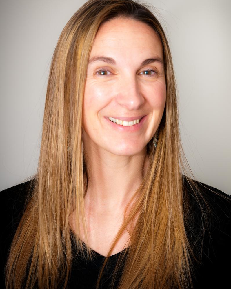 Edith Beigne合作论文数Meta12
 Bertrand Pelloux-Prayer合作论文数11
 Julien Le Coz合作论文数10Davide Rossi合作论文数9
 Jeanphilippe Noël合作论文数9
 Alexandre Valentian合作论文数CEA-LETI9
 Antonio Pullini合作论文数Politecnico di Torino9
 Luca Benini合作论文数Institut fur Integrierte Systeme, Eidgenossische Technische Hochschule Zurich;Department of Information Technology and Electrical Engineering, Eidgenossische Technische Hochschule Zurich9Bastien Giraud合作论文数8
 Milovan Blagojevic合作论文数7
 Borivoje Nikolic合作论文数Department of Electrical Engineering and Computer Sciences, University of California at Berkeley;Berkeley Wireless Research Center, University of California at Berkeley7Vincent Huard合作论文数STMicroelectronics Research and Development Center, Crolles7
 Olivier Thomas合作论文数6
 Sylvain Clerc合作论文数STMicroelectronics6Franck Arnaud合作论文数6
 Sylvain Engels合作论文数STMicroelectronics Central CAD S Design Solutions6
 Igor Loi合作论文数University of Bologna6
 Michael Gautschi合作论文数ETH Zurich5
 Mario R. Casu合作论文数Dept Elect & Telecommun, Politecn Torino5
 Robin Wilson合作论文数5
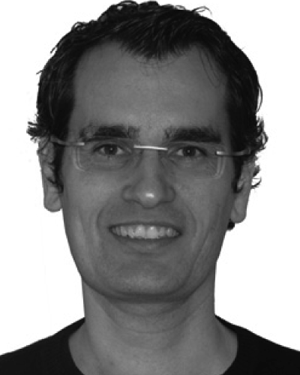 Ivan Miro-Panades合作论文数French Atomic Energy Commission5Sebastien Haendler合作论文数5
 Yvain Thonnart合作论文数CEA LETI FR5M BELLEVILLE合作论文数4o thomas合作论文数4Brian Zimmer合作论文数NVIDIA Corp4
 Ben Keller合作论文数4
 Anuj Grover合作论文数4
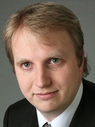 Andreas Peter Burg合作论文数Telecommunications Circuits Lab, École polytechnique fédérale de Lausanne;RAAAM Memory Technologies4
 Frank K. Gürkaynak合作论文数Integrated Systems Laboratory, Swiss Federal Institute of Technology4Vincent Liot合作论文数4
 Fady Abouzeid合作论文数STMicroelectronics4
 Marc Belleville合作论文数4B. Giraud合作论文数3P. Roche合作论文数3
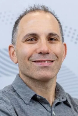 Adam Teman合作论文数Emerging Nanoscaled Integrated Circuits and Systems Labs, The Alexander Kofkin Faculty of Engineering, Bar Ilan University3
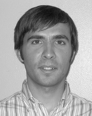 gilles gasiot合作论文数3
 Alfio Di Mauro合作论文数ETH3
 D'Agostino, C.合作论文数STMicroelectronics;c;STMicroelectronics3
 Jaehwa Kwak合作论文数3Pifeng Chiu合作论文数3
 Po-Hung Chen合作论文数3
 Krste Asanovic合作论文数Graduate School, Computer Science Division, EECS Department, University of California, Berkeley3
 Elad Alon合作论文数Department of Electrical Engineering and Computer Sciences, University of California, Berkeley;Berkeley Wireless Research Center, University of California, Berkeley3
 Pascal Nouet合作论文数University of Montpellier3
 Hanh-Phuc Le合作论文数College of Engineering & Applied Science, University of Colorado Boulder;Center for Wireless Communications, Jacobs School of Engineering, University of California, San Diego3
 Philippe Magarshack合作论文数3
 Alberto Puggelli合作论文数University of California3Nicolas Planes合作论文数STMicroelectronics3




