Magnetic resonance imaging (MRI) exhibits rich and clinically useful endogenous contrast mechanisms, which can differentiate soft tissues and are sensitive to flow, diffusion, magnetic susceptibility, blood oxygenation level, and more. However, MRI sensitivity is ultimately constrained by Nuclear Magnetic Resonance (NMR) physics, and its spatiotemporal resolution is limited by SNR and spatial encoding. On the other hand, miniaturized implantable sensors offer highly localized physiological information, yet communication and localization can be challenging when multiple implants are present. This paper introduces the MRDust, an active "contrast agent" that integrates active sensor implants with MRI, enabling the direct encoding of highly localized physiological data into MR images to augment the anatomical images. MRDust employs a micrometer-scale on-chip coil to actively modulate the local magnetic field, enabling MR signal amplitude and phase modulation for digital data transmission. Since MRI inherently captures the anatomical tissue structure, this method has the potential to enable simultaneous data communication, localization, and image registration with multiple implants. This paper presents the underlying physical principles, design tradeoffs, and design methodology for this approach. To validate the concept, a 900 $\times$ 990 $\mu$m${}^{2}$ chip was designed using TSMC 28 nm technology, with an on-chip coil measuring 630 $\mu$m in diameter. The chip was tested with custom hardware in an MR750W GE3T MRI scanner. Successful voxel amplitude modulation is demonstrated with Spin-Echo Echo-Planar-Imaging (SE-EPI) sequence, achieving a contrast-to-noise ratio (CNR) of 25.58 with a power consumption of 130 $\mu$W.
This paper presents a feedforward nonlinear equalizer (FFNE) framework for short- to medium-reach wireline links that removes the feedback-timing bottleneck of decision-feedback equalizers (DFEs) while approaching the noise-margin advantage within a characterized operating region. The proposed FFNE reduces short-window maximum-likelihood sequence estimation to a compact binary decision rule, enabling a low-complexity feedforward realization without transmitter-side encoding. For the single-postcursor NRZ case, the mathematical foundation, hardware implementation, tap adaptation, statistical analysis, and equalization limit relative to an ideal 1-tap DFE are established. A window-length-3 FFNE quantifies the performance-complexity tradeoff of longer sequence windows. The framework is further extended to PAM-4 modulation and simultaneous precursor/postcursor equalization through a pattern-detection-based FFNE (PD-FFNE), which outperforms conventional FFE+DFE baselines under representative channel conditions.
We present an LC-based hybrid sub-sampling phase-locked loop (PLL). A novel tri-state integral path is applied to reduce the loop filter (LF) area and eliminate ripples on the control signals. The effectiveness of the proposed technique is compared with type-II hybrid PLL and PLL using delta-sigma modulator. The 24.6-29.6GHz PLL instance implemented in 28-nm planar process achieves RMS jitter of 44fs and -254.8dB FOM and consumes power of 17mW from a 0.9/0.95V supply.
This article introduces a cascaded sliding-block decision feedback equalizer (SB-DFE) that equalizes multiple precursor and postcursor intersymbol interference (ISI). The paper also presents an enhanced statistical analysis for the DFE in the presence of residual ISI and additive white Gaussian noise (AWGN), along with generalized expressions for the probability and expected length of DFE burst errors. In addition, the statistical analysis is extended to the conventional SB-DFE and our proposed cascaded SB-DFE to accurately estimate their equalization capability, latency, and steady-state bit error rate (BER). The simulation results reveal that the cascaded SB-DFE provides as low BER as the mininum mean-squared error - DFE (MMSE-DFE) with substantially lower latency and hardware overhead.
This work presents a RISC-V system-on-chip (SoC) with eight application cores containing programmable-precision vector accelerators. The SoC is built by using a generator-based design methodology, which enables the integration of open-source and project-specific building blocks to develop differentiated functionality. The digital component generators use Chisel, the analog component generators use the Berkeley Analog Generator (BAG), and the physical design flow is implemented with Hammer. The chip totals 125 M gates and is implemented in a 16-nm finFET process. The vector accelerator achieves peak energy efficiency per task of 209 half-precision, 92 single-precision, and 56 double-precision GFLOPs/W for a matrix multiplication kernel at 0.55 V and 339 MHz.
This paper presents a complete 200Gb/s PAM-4 transmitter (TX) in 28nm CMOS technology. The transmitter features a hybrid sub-sampling PLL (SSPLL) with a delta-sigma (ΔΣ) modulator, clock distribution network with flexible timing control, and data path with a hybrid 5-tap Feed-Forward Equalizer (FFE) and T-coil for bandwidth extension. The prototype chip achieves 4.69 pJ/bit efficiency, 54mV eye height, 0.27UI eye width, and 97% RLM under ~6dB channel loss at 50GHz.
Growing demand for data across all communication requires an increase in both of capacity and density of back-haul point-to-point (PTP) and point-to-multipoint (PTMP) data links [1]. A D-band (110-170GHz) phased-array transceiver offers an attractive means to increase the capacity by leveraging the large available bandwidth and overcomes the high free-space path loss by adopting large array gain. Recent advances in process scaling are enabling > 100GHz transceiver implementations in low-cost CMOS technologies for commercial applications. In addition, to meet the requirements of future commercial systems above 100GHz, a low-cost and high-performance packaging platform is required. Recent publications have demonstrated high performance D-band transceivers capable of high-order and wide-bandwidth modulation [1, 2, 3, 4, 5]. However, very few are packaged or are tested with an on-chip PLL.
We present a ring-oscillator-based sub-sampling phase-locked loop (PLL) using a generator-based design flow. A hybrid loop with a delta-sigma ($\Delta \Sigma$) modulator is applied to reduce the loop filter (LF) area and the control ripple. The generator automatically produces the ring oscillator and PLL to meet the provided specifications. The 10-GHz PLL instance implemented in 28-nm planar process achieves RMS jitter of}299.5 fs and power of 9.9 mW from a 1-V supply.
This article presents a 200-Gb/s pulse amplitude-modulation four-level (PAM-4) and 100-Gb/s non-return-to-zero (NRZ) transmitter (TX) in 28-nm CMOS technology. To achieve the target data rate, the output bandwidth and swing of the proposed TX are optimized by minimizing the output capacitance of the 4:1 multiplexer (MUX) and driver stage with pull-up current sources and adopting a fully reconfigurable 5-tap feed-forward equalizer (FFE). The key circuit includes a segmented 8:4 MUX and 4:1 MUX/driver, a thermal encoder and retimer, and a flexible clock distribution network. Using the layout generated with Berkeley Analog Generator (BAG), the proposed TX achieves an eye opening with >52.9-mV eye height, 0.36 UI eye width, >98% RLM, and 4.63 pJ/b at 200-Gb/s PAM-4 signaling under >6-dB channel loss at 50 GHz, demonstrating the highest data rate achieved using a planar process.
LAYout with Gridded Objects (LAYGO), a Python-based layout-generation engine for enhancing the design productivity of custom circuit layouts in advanced CMOS processes, is presented and verified by implementing a time-interleaved SAR (TI-SAR) ADC instance in a 16 nm CMOS FinFET technology. LAYGO supports rapid generation by placing customized templates on process-specific placement grids, thereby encapsulating the design rules and process-specific structures. The templates can be located based on their relative positional information, which further enhances the description capability and portability. Interconnecting wires are routed on the grids for design rule abstractions, with additional customizations and support for multi-patterning. The functions for the on-grid placement and routing use advanced indexing and slicing with multi-dimensional object containers to improve the description and parameterization capabilities. Multiple TI-SAR ADC layouts are generated using LAYGO in 28-16 nm CMOS technologies. One instance is fabricated in a 16 nm CMOS FinFET process and measured, achieving a 38.2 dB signal-to-noise-and-distortion ratio (SNDR) at 7 GS/s after digital calibration and consuming 45.2 mW. Owing to its high customization capability, the design achieved the highest sampling rate (7 GS/s) among the generated ADCs.
This article presents a 71–86 GHz 16-element array receiver application-specified integrated circuit (ASIC) for Massive multiple-input–multiple-output (MIMO) wireless uplink, featuring a multiple-output analog beamformer (BF) supporting up to 16 spatially multiplexed users at the same time. The ASIC includes 16 direct-conversion mixer-first RX front-ends, local oscillator (LO) generation and distribution, and a $16\times 16$ fully connected baseband analog beamformer, which derives each user stream as a linear combination of all the 16 antennas. The 16 mm 2 28 nm CMOS ASIC is packaged on an organic interposer including a linear patch antenna array. Over-the-air measurements demonstrate up to 2 Gb/s single-user data-rate, and four simultaneous links at 500 Mb/s each, with number of users and data rate only limited by setup constraints. Circuits are optimized for low power consumption in order to enable scaling to massive arrays, and consumes 1.7 W total power, for a power figure of 7 mW/antenna/user.
The ever-expanding demand for ultra-high-speed interconnects has driven the development of wireline TXs operating at >100Gb/s per lane [1]-[4]. This paper presents a PAM-4 TX achieving 200Gb/s with improved output bandwidth and output swing by minimizing the driver capacitance with pull-up current sources, multiplexing with flexible clock timing control, and employing a fully reconfigurable 5-tap FFE architecture.
This work presents a 16mm2 heterogeneous RISC-V system-on-a-chip (SoC) composed of a high-performance out-of-order core, energy-efficient in-order core, data-parallel vector accelerator, and systolic array deep neural network (DNN) accelerator in low-power Intel 22FFL for general-purpose compute, DNN, and vector workloads. The heterogeneous RISC-V SoC is composed of fully open-source components, including a second-generation Berkeley Out-of-Order Machine (BOOM) with a non-speculative mode attached to a Hwacha vector accelerator, a Rocket in-order core attached to a Gemmini systolic array DNN accelerator, as well as a IMiB L2 cache and off-chip I/Os. Combined, the variety of heterogeneous compute allows for wide programmability while providing up to a 286x MOPS/W improvement or 282x MOPS improvement over the RISC-V in-order core.
Modern workloads, such as deep neural networks (DNNs), increasingly rely on dense arithmetic compute patterns that are ill-suited for general-purpose processors, leading to a rise in domain-specific compute accelerators [1]. Many of these workloads can benefit from varying precision during computation, e.g. different precisions among layers and between training and inference for DNNs has been shown to improve energy efficiency [2].
This brief discusses the limitation of previously published statistical decision feedback equalizer (DFE) models when residual inter-symbol interference (ISI) is present and proposes a method that overcomes this limitation. The paper presents an accurate closed-form expression for the DFE with residual ISI and additive white Gaussian noise (AWGN). The analysis is extended to 4-level pulse amplitude modulation (PAM-4) to cover serial links of current interest. The results verify that the proposed model estimates an accurate bit error rate (BER).
Multi-User MIMO (MU-MIMO) at mm-wave is a promising technique for high-capacity wireless access. A base-station array of M antennas simultaneously steers K independent beams, which enables spatial multiplexing and channel bandwidth reuse across multiple users. It has been shown that for M≫K (i.e. massive MIMO), linear algorithms can achieve near-optimal user tracking and spatial interference rejection [1]. The power and area demands of massive arrays are minimized with a fully connected architecture, where each beam is a combination of all available array elements [2]. However, a massive fully connected array results in significant hardware complexity.
We present a bang-bang phase-locked loop (PLL) generator that encapsulates design methodologies for its circuit blocks and the complete PLL system. The generator is fully automated and parameterized, producing the layout and schematic based on process characterization and top-level specifications. Three 14GHz PLLs are instantiated in TSMC 16nm, GF 14nm and Intel 22nm technologies, demonstrating the process portability. The rapid generation time of less than four days enables fast PLL design and technology porting. The PLL design fabricated in TSMC 16nm shows RMS jitter of 565.4fs and power of 6.64mW from a 0.9V supply.
 Borivoje Nikolic合作论文数Department of Electrical Engineering and Computer Sciences, University of California at Berkeley;Berkeley Wireless Research Center, University of California at Berkeley47
 Ali Niknejad合作论文数Electrical Engineering & Computer Sciences, University of California, Berkeley36
 Jan M. Rabaey合作论文数Department of Electrical Engineering and Computer Sciences, University of California, Berkeley26
 Jae-Duk Han合作论文数Sch Elect Elect Engn, Yonsei Univ22
 Mark Horowitz合作论文数Department of Electrical Engineering, Stanford University;Department of Computer Science, School of Engineering, Stanford University20
 Tsu-Jae King Liu合作论文数College of Engineering, University of California, Berkeley18
 Nathan Narevsky合作论文数18
 Jose M. Carmena合作论文数Center for Neural Engineering and Prostheses, University of California, Berkeley;Department of Electrical Engineering and Computer Sciences, University of California, Berkeley17
 Zhongkai Wang合作论文数Univ Calif Berkeley, Berkeley, CA 94720 USA16
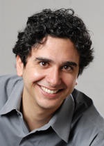 Michel Maharbiz合作论文数Berkeley Sensor & Actuator Center, University of California, Berkeley;Center for Neural Engineering & Prostheses, University of California, Berkeley;Department of Electrical Engineering and Computer Science, University of California, Berkeley;TweedleTech;Iota Biosciences, Inc.;Cortera Neurotechnologies, Inc.16
 Lingkai Kong (孔令恺)合作论文数Harvard University15
 Krste Asanovic合作论文数Graduate School, Computer Science Division, EECS Department, University of California, Berkeley14
 Hei Kam合作论文数Apple14
 Dongjin Seo合作论文数Neuralink13
 Nicholas Sutardja合作论文数12
 Vladimir Stojanovic合作论文数Berkeley Wireless Research Center, University of California, Berkeley;Center for Energy Efficient Electronics Science, University of California, Berkeley;Berkeley Emerging Technologies Research Center, University of California, Berkeley12
 Stevo Bailey合作论文数11
 Rhesa Nathanael合作论文数University of California11
 Jaeseok Jeon合作论文数Dept Elect Engn & Comp Sci, Univ Calif Berkeley11
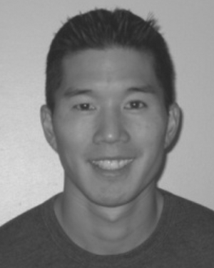 Fred Chen合作论文数11
 Vincent Pott合作论文数10
 Brian C. Richards合作论文数Department of Electrical Engineering and Computer Sciences, University of California at Berkeley10
 Ron Ho合作论文数Meta10
 Antonio Puglielli合作论文数Berkeley Wireless Research Center, University of California, Berkeley, CA, USA9
 Angie Wang合作论文数Department of Electrical Engineering and Computer Sciences, University of California9
 Dinesh Patil合作论文数9
 Eric I-Chao Chang (張益肇)合作论文数AI + Health Startups9
 Hanh-Phuc Le合作论文数College of Engineering & Applied Science, University of Colorado Boulder;Center for Wireless Communications, Jacobs School of Engineering, University of California, San Diego9
 Andrew Ho合作论文数9
 Greg LaCaille合作论文数8
 Minsoo Choi合作论文数8
 Milovan Blagojevic合作论文数8
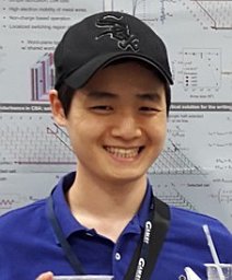 Woorham Bae合作论文数8
 Alberto Puggelli合作论文数University of California8
 Kwangmo Jung合作论文数Berkeley Wireless Research Center, University of California, Berkeley8
 Frankie Liu合作论文数8
 Colin T. A. Schmidt合作论文数8
 Kyoungtae Lee合作论文数University of California at San Francisco7
 Ayan Biswas合作论文数Univ Calif Berkeley, Berkeley, CA 94720 USA7Brian Zimmer合作论文数NVIDIA Corp7
 Ben Keller合作论文数7
 Jaehwa Kwak合作论文数7Pifeng Chiu合作论文数7
 Jonathan Bachrach合作论文数JITx7Jon Lexau合作论文数7
 Yunsup Lee合作论文数SiFive, Inc.7
 Ruzica Jevtic Novakovic合作论文数Departamento de Ingeniería Electrónica, Universidad Politécnica de Madrid7
 Zhaokai Liu合作论文数Univ Calif Berkeley, Berkeley, CA 94720 USA6
 John Wright合作论文数Univ Calif Berkeley, Berkeley, CA 94720 USA6